The Missing Architectural Piece
After months of building discrete logic components in isolation—counters, memory interfaces, basic sequencers—the DINO CPU project had stalled at a fundamental level. Individual subsystems functioned correctly, but coordinating them into a working computer remained an elusive challenge. What I had dismissed as “simple switching logic” revealed itself as the most critical architectural component: systematic control coordination.
The breakthrough came from stepping away from ad-hoc circuit assembly and studying proven computer architecture principles. Paul Malvino’s ( “Digital Computer Electronics” ) SAP-1 design provided the methodical approach my discrete logic implementation was missing.
From Chaos to Coordination
Previous attempts used SPDT switches and basic gate logic to coordinate bus access and memory operations. This approach worked for simple demonstrations but failed when multiple devices needed precise timing coordination. The fundamental issue wasn’t component selection—it was control system architecture.
Real computers require systematic control word generation, not intuitive switching circuits. The control unit acts as conductor, orchestrating fetch-decode-execute cycles through precisely timed signal coordination.
Ring Counter Implementation Discovery
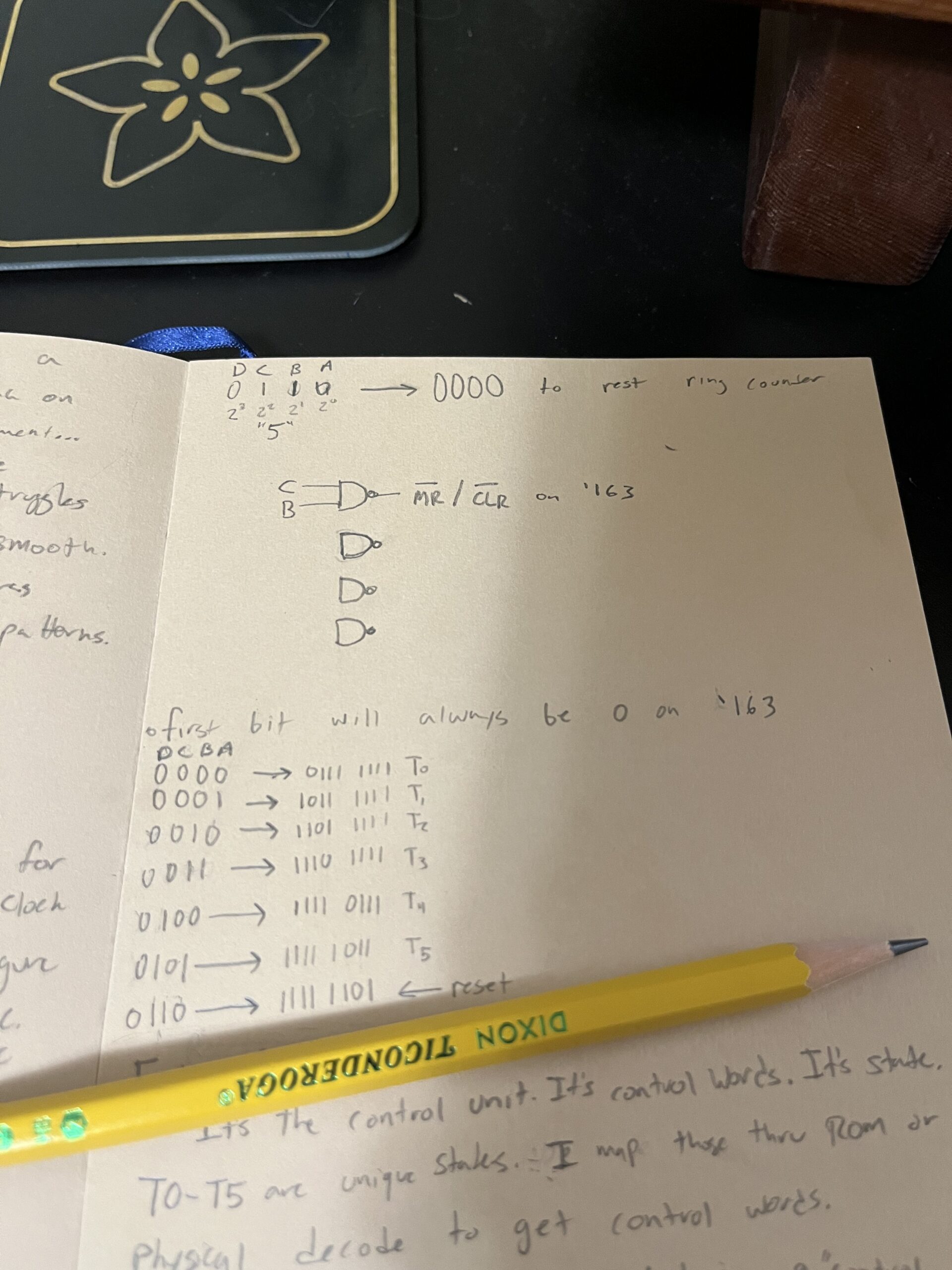
SAP-1’s control timing depends on sequential states T0→T1→T2→T3→T4→T5→T0 that coordinate instruction phases. Initial component research focused on 74LS164 shift registers, but availability constraints demanded alternative approaches.
The solution emerged from standard TTL components:
- 74S163: 4-bit synchronous counter (binary sequence 0-5, then reset)
- 74LS138: 3-to-8 decoder (converts binary count to one-hot timing signals)
- 74LS00: NAND gate (detects count=6 to trigger reset)
Reset Logic: When the counter reaches binary 110 (decimal 6), both QB and QC outputs go HIGH. The NAND gate detects this condition and outputs LOW, triggering the 163’s active-low CLR input. The counter immediately resets to 000, creating the ring behavior.
Truth Table Verification: The 74LS138 decoder creates exactly the one-hot sequence required:
Counter Input → Decoder Output (Active LOW)
000 → Y0 (T0 timing state)
001 → Y1 (T1 timing state)
010 → Y2 (T2 timing state)
011 → Y3 (T3 timing state)
100 → Y4 (T4 timing state)
101 → Y5 (T5 timing state)
Control Word Architecture Breakthrough
The ring counter provides timing states, but SAP-1’s intelligence comes from translating those states into specific control operations. Each timing state generates an 8-bit control word that enables or disables specific system functions.
Universal Fetch Cycle (T0-T2):
- T0: Program counter drives address bus, memory read enabled
- T1: Increment program counter
- T2: Load instruction register from data bus
Instruction-Specific Execute Cycle (T3-T5):
- Varies by instruction type (LDA, ADD, OUT, etc.)
- Different control signals active based on operation requirements
- Same timing framework, different control word patterns
ROM-Based Control Matrix: Instead of implementing Malvino’s discrete gate logic, modern EEPROM provides elegant lookup table functionality. Address formation combines instruction opcode with timing state: [Instruction bits][Timing state bits] = ROM address. The data at that address contains the exact control word needed for that specific (instruction, timing) combination.
Historical Perspective
This revelation sparked appreciation for the intellectual journey from abstract mathematics to physical computation. George Boole’s Boolean algebra (1854) provided the mathematical foundation, Claude Shannon’s switching theory thesis (1937) connected those abstractions to physical circuits, and now discrete TTL components implement those same principles on the breadboard.
It’s been a journey standing on the shoulders of giants who transformed pure logic into computational reality.
Engineering Insight
The control unit isn’t just another subsystem—it’s the architectural element that transforms individual components into a coordinated computer. Understanding this principle bridges the gap between discrete logic experimentation and real processor design fundamentals.
Modern processors use identical fetch-decode-execute principles, just implemented in silicon with enhanced complexity. The same control timing concepts scale from SAP-1’s 6 states to modern processors’ 15-20 pipeline stages.
Next Phase Implementation
With control timing architecture understood, the next development phase involves:
- Mapping complete data paths between SRAM, registers, ALU, and output systems
- Defining all control signal requirements and bus arbitration logic
- Implementing ROM-based control matrix using 28C256 EEPROM
- Creating control word definitions for SAP-1’s basic instruction set
The control unit mystery has been solved. Now it’s systematic engineering execution to bring the discrete logic computer to life.