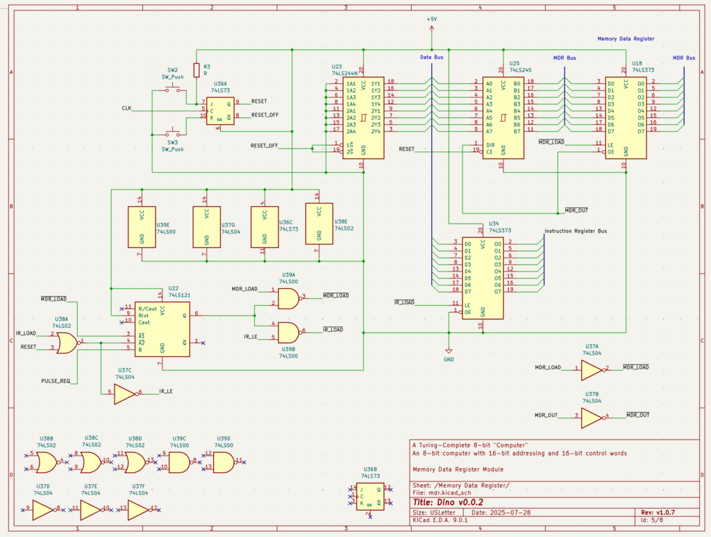
The Control Word Generation Module
Following the completion of the Program Counter module, the next critical milestone in the DINO CPU build was implementing the Microcode Decoder Module. This subsystem is the decoding bridge between the Program Counter, Instruction Register, and datapath — transforming a simple count and timing phases into precise sequences of control signals that orchestrate the CPU’s fetch–decode–execute cycle.
This marks a shift in the project’s pace: we are now working with deliberate, methodical engineering discipline. No longer in discovery mode, each module is designed on paper, validated logically, then wired and tested against clearly defined criteria before being declared operational.
Architectural Role
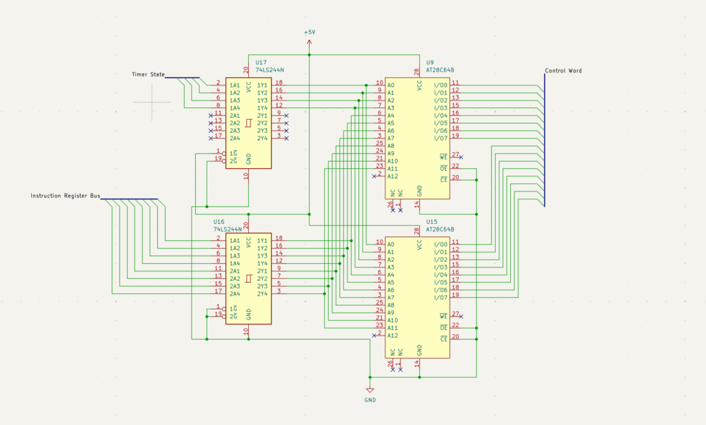
The Microcode Decoder accepts:
- Timer Phase from the ring counter
- Instruction Opcode from the Instruction Register
These form a 16-bit address into a parallel EEPROM pair:
- ROM #1: upper byte
- ROM #2: lower byte
Example: address 0xBEEF would store 0xBE in ROM #1 and 0xEF in ROM #2. The output directly drives the control lines of the CPU via decoder banks, enabling deterministic hardware sequencing.
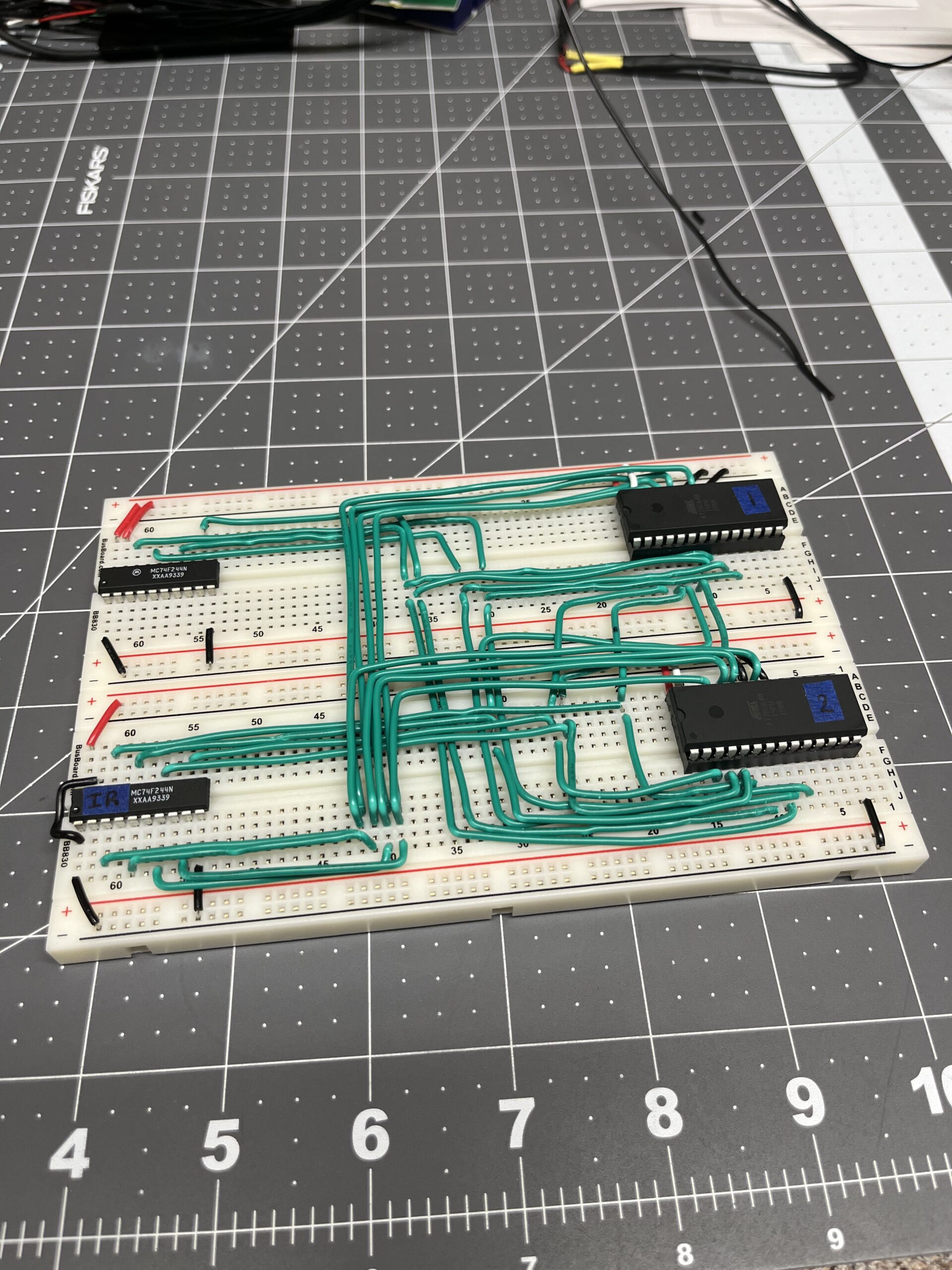
Hardware Selection
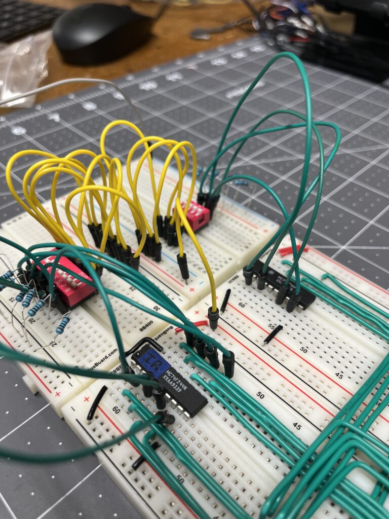
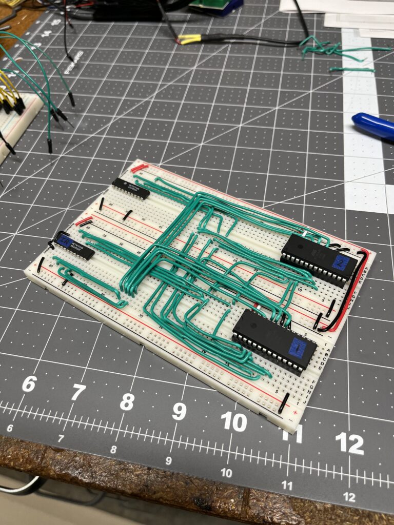
- ROMs: 2 × AT28C64 8-KB EEPROMs, wired in parallel for 16-bit output
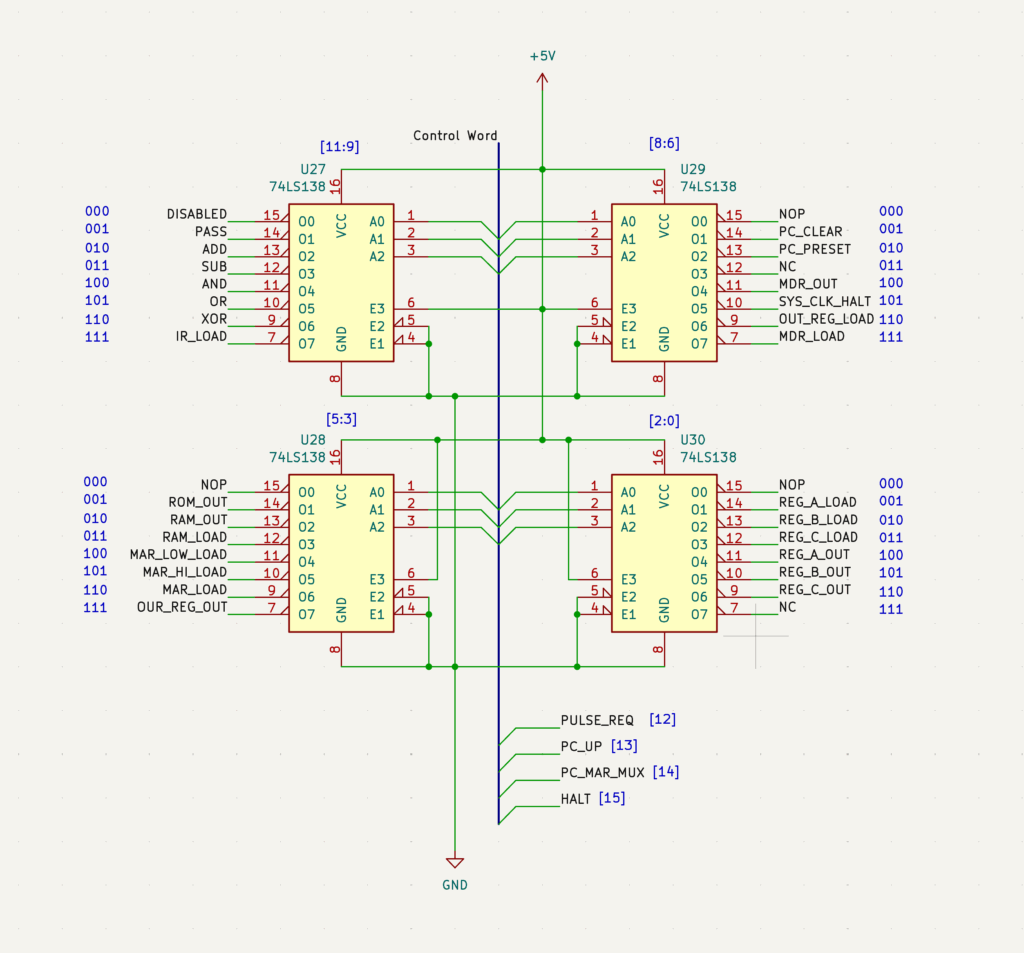
- Decoders: 4 × 74LS138N 3-to-8 demultiplexers to split the 16 control word bits into functional banks, with 4 additional lines reserved for signals that are not mutually exclusive with other control bits.
- Pulse Generation: 74LS121 monostable multivibrators for intra-phase latching
ISA Revision and Bit-Ordering Correction
Early in design, the instruction set was built with the first bit as MSB, but the hardware required it as LSB. Correcting this forced schematic revisions, but clarified the logical flow from opcode to control word.
Current Instruction Set:
LDAI, LDBI, STA, STB, NOP, LDA, ADD, MOV, OUT, HLTThese instructions form the minimum set needed to verify memory transfers, register operations, arithmetic, and output control.
Control Word Matrix
The Microcode Decoder produces a 16-bit control word, organized into functional groups:
| Bit(s) | Function / Decoder Bank | Codes & Meanings |
|---|---|---|
| 15 | HALT | Start the next phase early |
| 14 | MAR_PC_MUX | Use MAR or PC as address source for IR |
| 13 | PC_UP | Increment Program Counter |
| 12 | PULSE_REQ (new) | Intra-phase pulse trigger |
| 11:9 | Bank 4: ALU Ops | 000: ALU Disabled 001: Pass Accumulator 010: ADD 011: SUB 100: AND 101: OR 110: XOR 111: IR_LOAD |
| 8:6 | Bank 3: Program Counter Control | 000: NOP 001: PC_CLEAR 010: PC_PRESET 011: unused 100: MDR_OUT 101: SYS_HALT 110: OUT_REG_LOAD 111: unused |
| 5:3 | Bank 2: Memory Ops | 000: NOP 001: ROM_OUT 010: RAM_OUT 011: RAM_LOAD 100: MAR_LO_LOAD 101: MAR_HI_LOAD 110: MAR_LOAD 111: OUT_REG_OUT |
| 2:0 | Bank 1: Register Ops | 000: NOP 001: REG_A_LOAD 010: REG_B_LOAD 011: REG_C_LOAD 100: REG_A_OUT 101: REG_B_OUT 110: REG_C_OUT 111: MDR_LOAD |
The PULSE_REQ Discovery
While defining the control word matrix, it became clear that certain latch operations could not reliably complete within a full T-phase. Halting and latching data simultaneously left uncertainty about whether the latch would capture stable data.
Solution: Introduce an intra-phase pulse (PULSE_REQ) generated by a 74LS121 to trigger latches early enough for guaranteed stability — essential for RAM writes and 74LS373 register loads.
Boot Sequence Strategy
- Microcode Addresses 0x0000–0x000F: Reserved for boot sequence
- Reset mode forces opcode
0x00into the IR via a 74LS244 buffering hardwired zeros - JK flip-flop (74LS73) keeps the opcode at
0x00until reset mode is released - At
0x0000: Microcode resets the PC - At
0x000F: PC is incremented - IR loads new opcodes only after reset mode ends
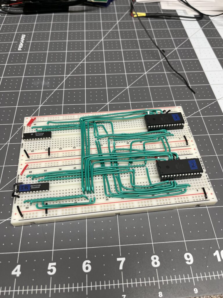
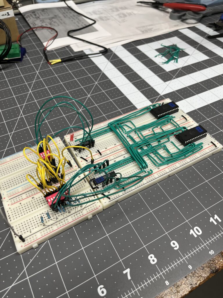
Schematic Development
The Microcode Decoder and the next modules (MDR, IR, Memory, Registers) have been fully drafted in KiCAD to ensure logical consistency before wiring.
Test Strategy
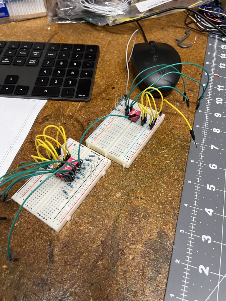
Testing verified correct EEPROM byte pairing for given addresses. DIP switches simulated opcode + timer phase. A multimeter was used to measure each ROM output pin, as the static conditions made it easier than a logic analyzer. Measurements were recorded in the engineering journal and compared to expected binary/hex values.
Test steps:
- Set DIP switches for desired address
- Measure each ROM output with multimeter
- Record voltage levels, convert to binary/hex
- Compare with EEPROM binary file contents
- Repeat for all patterns
| Address | ROM #1 (High Byte) | ROM #2 (Low Byte) |
|---|---|---|
| 0x0000 | 0xDE | 0xAD |
| 0x0001 | 0xBE | 0xEF |
| 0x0DED | 0xBE | 0xEF |
| 0x0FED | 0xFE | 0xED |
Two C programs supported test and verification:
test.c
/**
 * test.c - Parallel EEPROM test data generator for DINO
 *
 * This program generates two binary files (eeprom1.bin and eeprom2.bin)
 * for burning into two parallel EEPROMs used in the DINO hardware project.
 *
 * Each file is 4096 bytes (0x1000) and specific values are written at key addresses:
 *   - eeprom1.bin: 0xDE at 0x0000, 0xBE at 0x0001, 0xBE at 0x0DED, 0xFE at 0x0FED
 *   - eeprom2.bin: 0xAD at 0x0000, 0xEF at 0x0001, 0xEF at 0x0DED, 0xED at 0x0FED
 *
#
# Usage:
#   To compile:
#     gcc test.c -o test
#
#   To generate the EEPROM files:
#     ./test
#
#   To check the contents of each bin file:
#     hexdump -C eeprom1.bin
#     hexdump -C eeprom2.bin
#
#   How to read the output:
#     - The address at the start of each line (e.g., 00000fe0) is the starting offset for that line.
#     - Each line shows 16 bytes, so the first byte is at the line's address, the second at address+1, etc.
#     - To find a specific address (e.g., 0x0FED), calculate its position: 0x0FE0 + 13 = 0x0FED (13th byte in the line).
#     - Count bytes from left to right, starting at 0 for each line.
#     - Example: If you see 'fe' as the 13th byte on the line starting with 00000fe0, that's the value at 0x0FED.
#
 * All other bytes are zero-filled. This is for hardware and microcode testing.
 */
#include <stdio.h>
#include <stdint.h>

int main(void) {
    FILE *f1 = fopen("eeprom1.bin", "wb");
    FILE *f2 = fopen("eeprom2.bin", "wb");
    if (!f1 || !f2) {
        perror("Failed to open one of the files");
        if (f1) fclose(f1);
        if (f2) fclose(f2);
        return 1;
    }
    uint8_t eeprom1[0x2000] = {0};
    uint8_t eeprom2[0x2000] = {0};

    // Fill both EEPROMs with zeros
    for (int i = 0; i < sizeof(eeprom1); i++) {
        eeprom1[i] = 0x00;
        eeprom2[i] = 0x00;
    }

    // Write 0xDE at 0x0000 in eeprom1
    eeprom1[0x0000] = 0xDE;
    // Write 0xAD at 0x0000 in eeprom2
    eeprom2[0x0000] = 0xAD;

    // Write 0xBE at 0x0001 in eeprom1
    eeprom1[0x0001] = 0xBE;
    // Write 0xEF at 0x0001 in eeprom2
    eeprom2[0x0001] = 0xEF;

    // Write 0xBA at 0x0002 in eeprom1
    eeprom1[0x0002] = 0xBA;
    // Write 0xBE at 0x0002 in eeprom2
    eeprom2[0x0002] = 0xBE;

    // Write 0xBE at 0x0DED in eeprom1
    eeprom1[0x0DED] = 0xBE;

    // Write 0xEF at 0x0DED in eeprom2
    eeprom2[0x0DED] = 0xEF;

    // Write 0xCA at 0x0003 in eeprom1
    eeprom1[0x0003] = 0xCA;
    // Write 0xFE at 0x0003 in eeprom2
    eeprom2[0x0003] = 0xFE;

    // Write 0xFE at 0x0FED in eeprom1
    eeprom1[0x0FED] = 0xFE;
    // Write 0xED at 0x0FED in eeprom2
    eeprom2[0x0FED] = 0xED;

    fwrite(eeprom1, sizeof(uint8_t), sizeof(eeprom1), f1);
    fwrite(eeprom2, sizeof(uint8_t), sizeof(eeprom2), f2);
    fclose(f1);
    fclose(f2);
    return 0;
}
verify.c
/**
 * verify.c - Verifies specific addresses in eeprom1.bin and eeprom2.bin
 *
 * This program reads eeprom1.bin and eeprom2.bin, then prints the values at key addresses:
 *   - 0x0000, 0x0001, 0x0002, 0x0003, 0x0DED, 0x0FED
 *
 * Output format:
 *   EEPROM1[0xADDR] = 0xXX
 *   EEPROM2[0xADDR] = 0xXX
 *
 * Usage:
 *   gcc verify.c -o verify
 *   ./verify
 */
#include <stdio.h>
#include <stdint.h>
#include <stdlib.h>

#define EEPROM_SIZE 0x2000

int main(void) {
    const char *fname1 = "eeprom1.bin";
    const char *fname2 = "eeprom2.bin";
    FILE *f1 = fopen(fname1, "rb");
    FILE *f2 = fopen(fname2, "rb");
    if (!f1 || !f2) {
        perror("Failed to open one of the EEPROM files");
        if (f1) fclose(f1);
        if (f2) fclose(f2);
        return 1;
    }
    uint8_t eeprom1[EEPROM_SIZE];
    uint8_t eeprom2[EEPROM_SIZE];
    if (fread(eeprom1, 1, EEPROM_SIZE, f1) != EEPROM_SIZE) {
        fprintf(stderr, "Error reading %s\n", fname1);
        fclose(f1); fclose(f2);
        return 2;
    }
    if (fread(eeprom2, 1, EEPROM_SIZE, f2) != EEPROM_SIZE) {
        fprintf(stderr, "Error reading %s\n", fname2);
        fclose(f1); fclose(f2);
        return 3;
    }
    fclose(f1);
    fclose(f2);

    uint16_t addresses[] = {0x0000, 0x0001, 0x0002, 0x0003, 0x0DED, 0x0FED};
    size_t n = sizeof(addresses)/sizeof(addresses[0]);
    printf("EEPROM Verification Results:\n");
    for (size_t i = 0; i < n; ++i) {
        printf("EEPROM1[0x%04X] = 0x%02X\n", addresses[i], eeprom1[addresses[i]]);
        printf("EEPROM2[0x%04X] = 0x%02X\n", addresses[i], eeprom2[addresses[i]]);
    }
    return 0;
}
Burn & Verification
- EEPROMs written with a GECU T48 programmer via
minipro - ROM #1 programmed with high byte file, ROM #2 with low byte file
- Multiple rewire/re-burn cycles until outputs matched expected values
Milestone Achievement
The Microcode Decoder is fully functional. It bridges the Program Counter and upcoming MDR/IR stages, converting opcodes and timing into precise control signals for the CPU.
Engineering Methodology
This build reinforced:
- Correcting data representation early prevents cascading errors
PULSE_REQimproved timing integrity and latch reliability- Static signal verification with a multimeter can be more effective than a logic analyzer for certain tests
- Pre-drafting future modules ensures coherent datapath planning
Next Steps
- Memory Data Register (MDR) – temporary storage for memory read/writes
- Instruction Register (IR) – holds current opcode for decoding
- Memory Module & Register Module – completes the execution datapath