From Theory to Working Hardware
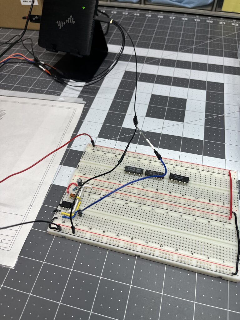
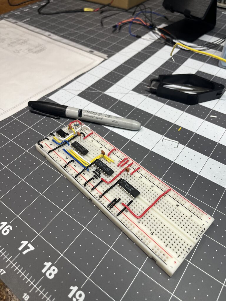
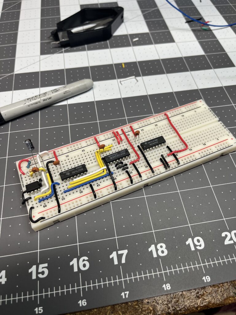
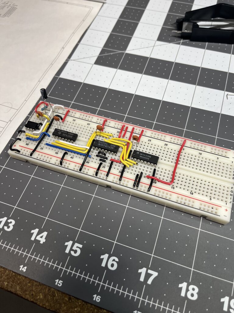
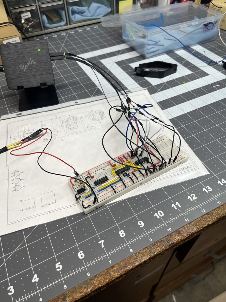
With the control unit revelation providing clear direction for systematic timing coordination, the next phase involved translating architectural understanding into working hardware. The ring counter represents the timing heart that enables control word coordination – transforming the theoretical framework into practical implementation.
The goal was to build the systematic T0-T5 timing sequence that would drive control word lookups and instruction execution phases.
Ring Counter Implementation
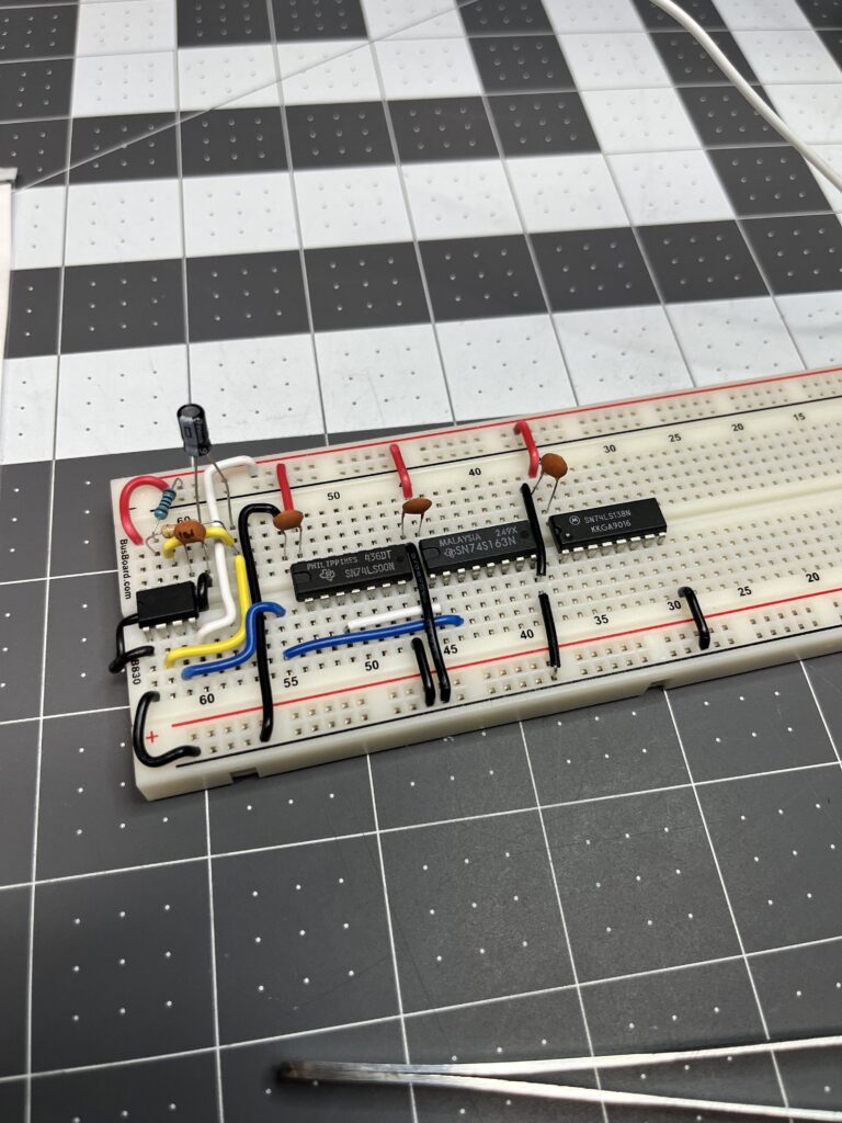
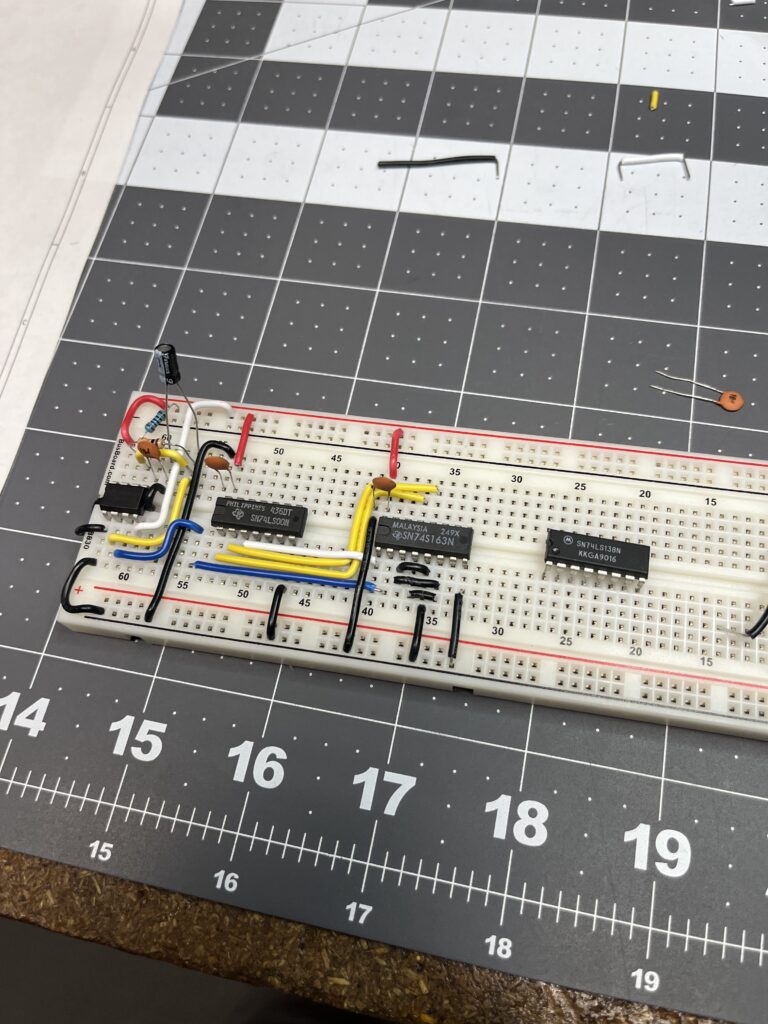
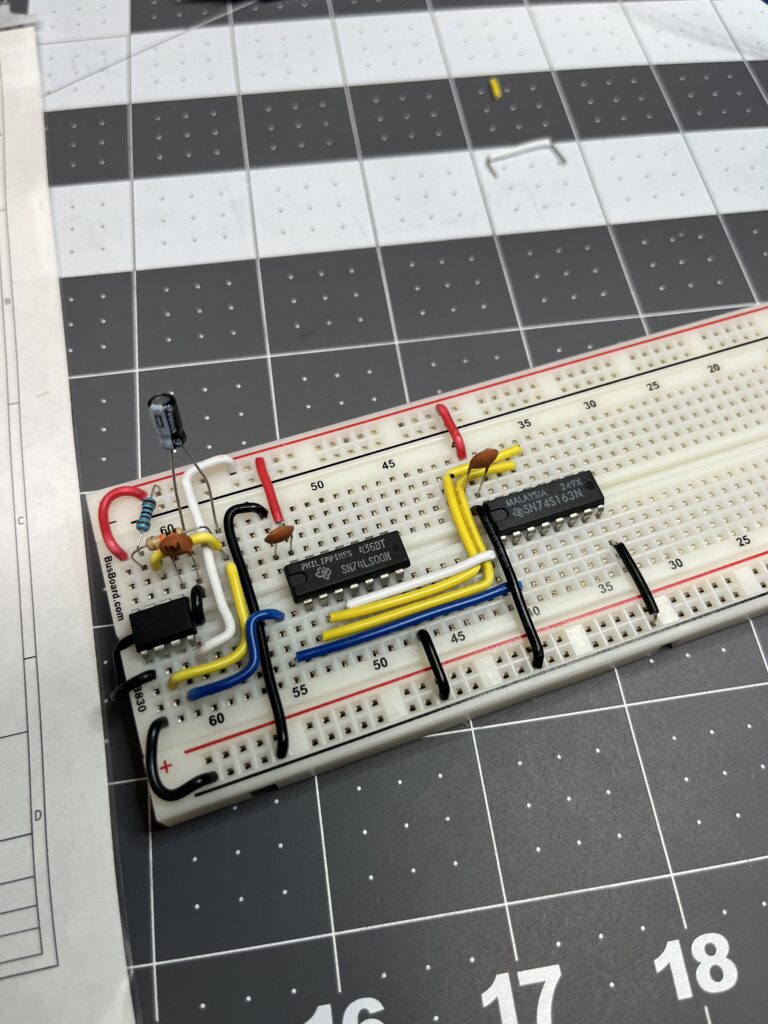
Hardware Components
- 74LS163: 4-bit synchronous counter (binary sequence generation)
- 74LS138: 3-to-8 decoder (converts binary count to one-hot timing signals)
- 74LS00: NAND gate (detects count=6 to trigger reset)
- NE555P: Timer circuit (proven from previous sequencer design)
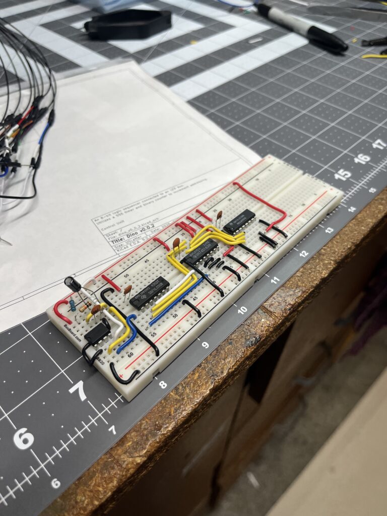
Circuit Operation
The implementation creates a systematic T0→T1→T2→T3→T4→T5→reset timing sequence:
Reset Logic: When the counter reaches binary 110 (decimal 6), both QB and QC outputs go HIGH. The NAND gate detects this condition and outputs LOW, triggering the ‘163’s active-low CLR input. The counter immediately resets to 000, creating the ring behavior.
Decoder Output Pattern: The ‘138 decoder creates the required one-hot sequence with active-low outputs:
000 (T0): Y0=LOW → 0111 1111001 (T1): Y1=LOW → 1011 1111010 (T2): Y2=LOW → 1101 1111011 (T3): Y3=LOW → 1110 1111100 (T4): Y4=LOW → 1111 0111101 (T5): Y5=LOW → 1111 1011
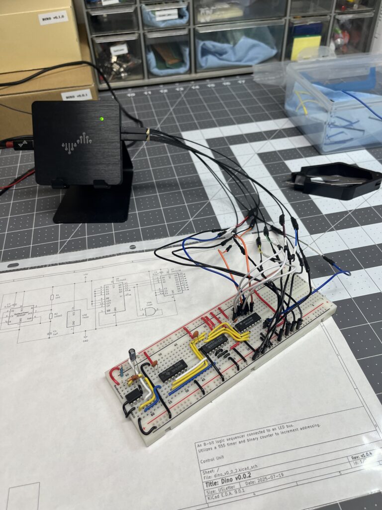
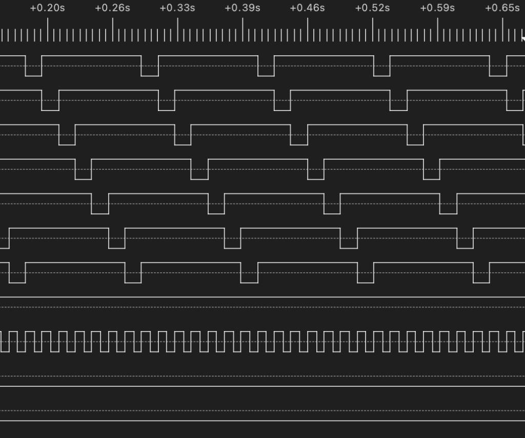
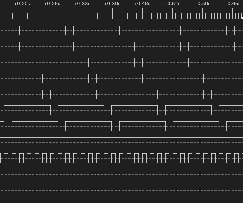
Logic Analyzer Validation
The ring counter was validated using logic analyzer capture, confirming:
- Six distinct timing states: Clean T0→T1→T2→T3→T4→T5 sequence
- Reset behavior: 7th state triggers reset pulse, immediately returns to T0
- Timing consistency: Each state lasts approximately 60ms (consistent with 555 timing)
- Signal integrity: Clean edges, proper logic levels, no glitches
- Stable operation: Continuous cycling without timing irregularities
The systematic T0-T5 timing states provide the foundation needed for control word generation and instruction sequencing.
Architecture Planning and Component Selection
Control Unit Evolution
The successful ring counter implementation enabled architectural planning for the complete control unit system:
Memory Architecture Defined:
- 0x0000-0x0FFF: Control word table (4KB)
- 0x1000-0xFFFF: Program space (60KB)
- Parallel AT28C256 ROMs: 16-bit control words and instructions
Instruction Register Implementation:
- Two 74LS373: 8-bit transparent latches configured for 16-bit instruction storage
- T1 control: LE signal derived from inverted T1 timing state
- Stable operation: Transparent during T1 (instruction fetch), latched during T2-T6 (execute)
Expandability Considerations
The current 6-state ring counter can be expanded to 7 states by changing the reset detection logic:
- Current: Detect count=6 (QB AND QC)
- Future: Detect count=7 (QB AND QC AND QD) using 74LS10 triple 3-input NAND
Engineering Methodology Validation
This implementation phase validated several critical embedded development practices:
- Component isolation testing: Ring counter validated independently before system integration
- Logic analyzer verification: Hardware-level visibility essential for timing validation
- Systematic problem resolution: Theoretical analysis confirmed by practical measurement
- Proven building blocks: Timer circuit preserved from working sequencer design
Next Phase Preparation
The ring counter milestone establishes the timing foundation for control word matrix implementation. With systematic T0-T5 timing generation validated, the next development phase involves:
- Control word architecture: ROM-based lookup table implementation
- Instruction register integration: 16-bit instruction storage and decode
- Data path coordination: Register, ALU, and memory interface control
The control unit timing heart is operational. The systematic approach from proven ring counter timing → control word architecture → complete CPU represents solid engineering methodology where each phase builds on validated previous work.
Memory Architecture Discovery
The ring counter implementation sparked investigation into memory organization and system architecture. Several key insights emerged:
Data Flow Architecture: The systematic data movement follows ROM→RAM→Register pathways rather than direct ROM→Register connections. This staging approach enables proper timing coordination where ROM data is first loaded into RAM workspace, then selectively moved to registers during appropriate timing states. SRAM provides the essential intermediate storage that allows the control unit to coordinate complex multi-step data transfers, while registers (74LS373) provide the parallel access needed for immediate decoder input and ALU operations.
Parallel ROM Configuration: Two AT28C256 ROMs configured in parallel create 32K × 16-bit memory space rather than 64KB total capacity. This configuration provides 16-bit instruction words and control words while maintaining single-address access. The parallel approach eliminates the complexity of interleaved addressing while maximizing control word capability.
Memory Map Strategy: Partitioning the 32K address space into control word table (0x0000-0x0FFF) and program storage (0x1000-0xFFFF) enables systematic ROM utilization. The same physical ROM serves dual purposes through address decoding – control unit accesses lower addresses for timing coordination while program counter accesses higher addresses for instruction fetch.
Pencil and Paper Phase
With the timing foundation established and memory architecture understood, the next development phase requires stepping away from hardware implementation to focus on systematic program design. The ring counter provides reliable timing coordination, but defining what instructions to execute demands careful planning:
Program Definition Requirements:
- Basic instruction set specification (LOAD, ADD, OUT, HALT, JMP)
- Control word definitions for each instruction timing phase
- Data flow coordination between ROM, RAM, registers, and ALU
- Memory organization for both program storage and control word lookup
The hardware platform can execute any systematic instruction sequence, but creating meaningful programs requires understanding what computational tasks the discrete logic system should demonstrate.
The transition from working timing hardware to systematic programming represents the shift from component validation to computer architecture implementation.