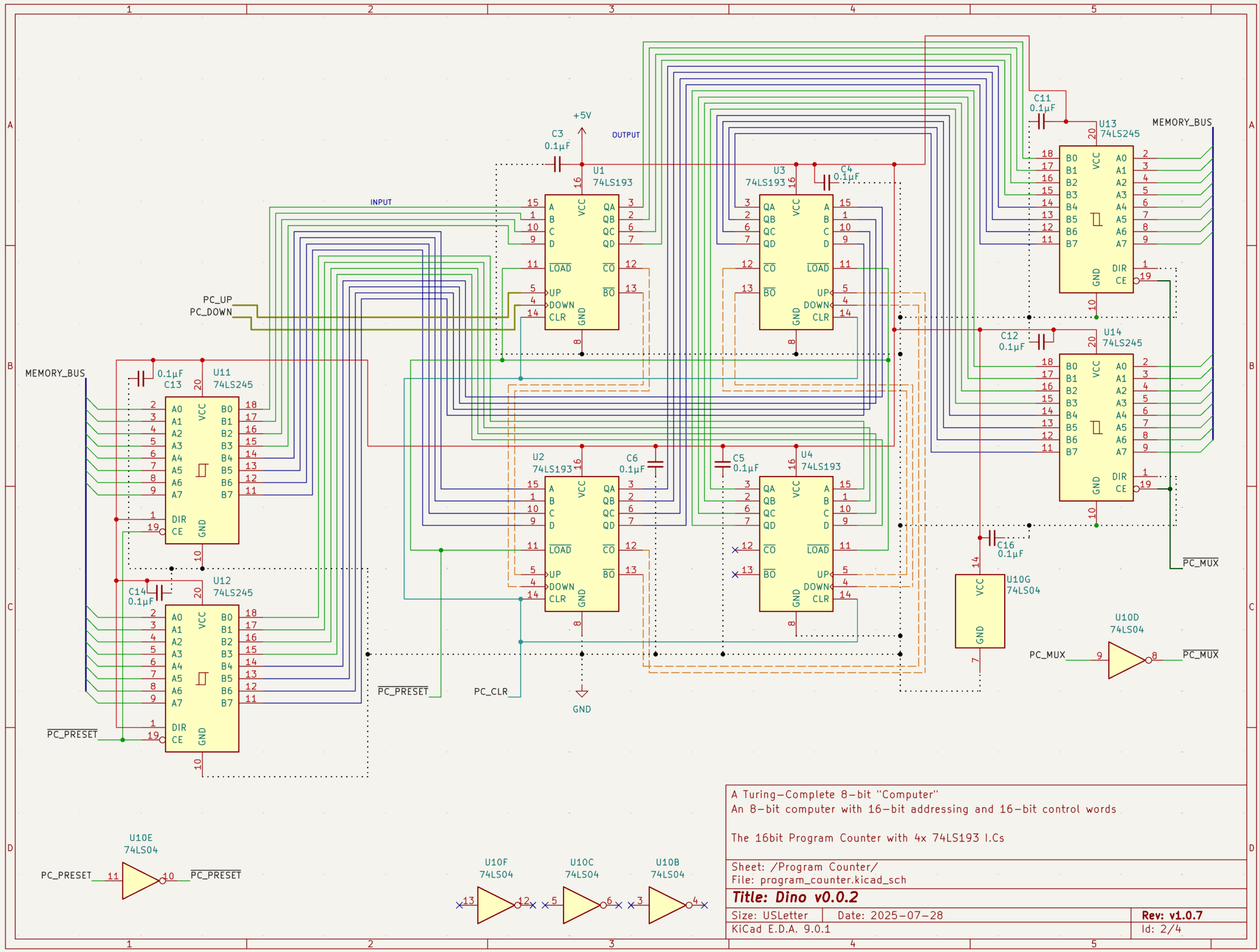
The Critical Address Generation Foundation
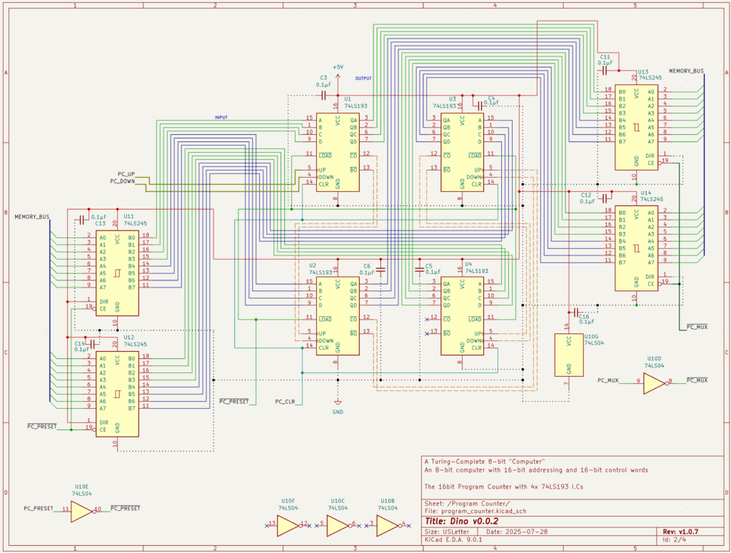
With the ring counter establishing systematic timing coordination, the DINO CPU project reached a pivotal engineering milestone: implementing the 16-bit Program Counter that would serve as the addressing backbone for all instruction execution. This module demanded cascaded counter logic with bidirectional operation, preset capability, and clean bus arbitration – functionality that would make or break the entire discrete logic computer.
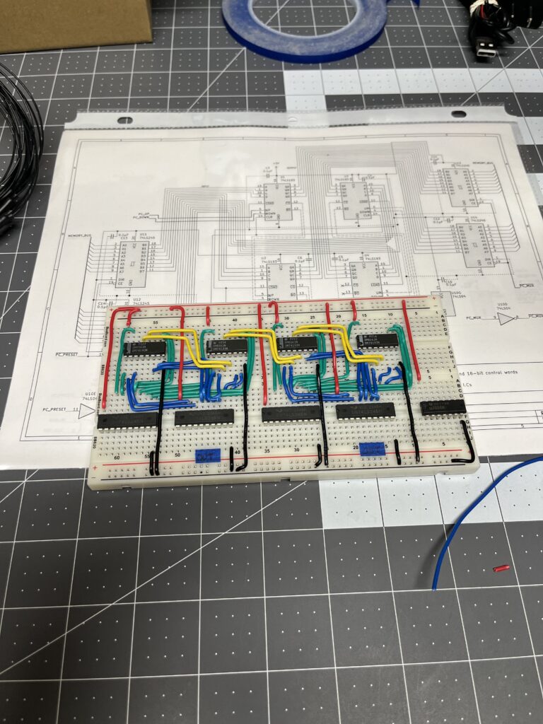
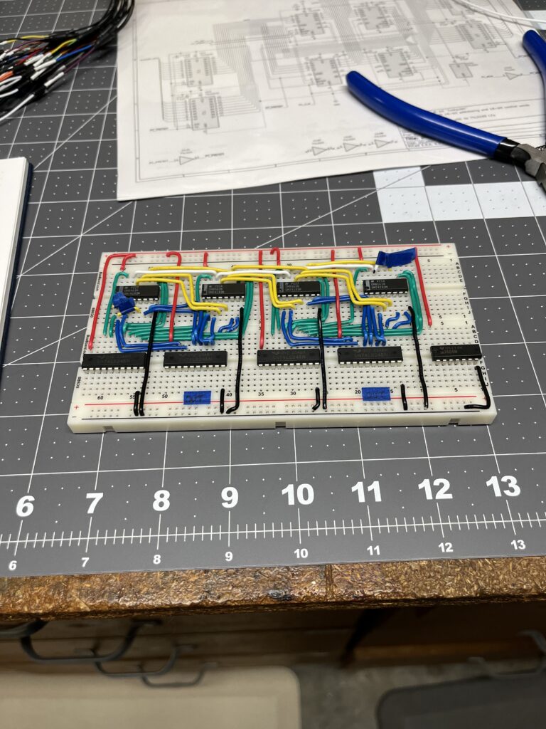
The engineering challenge centered on coordinating four 74LS193 counters through 74LS245 bus transceivers while maintaining signal integrity across a complex 16-bit address architecture.
Schematic Architecture and Component Analysis
Strategic Component Selection
The PC implementation required components that could handle complex addressing requirements:
- 74LS193 Quad Counters: Chosen for bidirectional counting with independent up/down clocks and comprehensive preset functionality
- 74LS245 Bus Transceivers: Essential for bidirectional bus control and output enable coordination
- 74LS02 NOR Gate: Provides active-low signal inversion required for control word compatibility
Circuit Complexity Evolution
The schematic development represented the most intricate circuit design attempted to date. Initial architecture included a 74LS32 OR gate for PC_MUX decode logic, but systematic analysis revealed this was redundant – the control word matrix already provided the necessary logic states.
This optimization eliminated unnecessary components while simplifying the signal routing:
- Iteration 1: Complete counter cascade with redundant decode logic
- Iteration 2: Streamlined design with OR gate removal and corrected DIR signals on output transceivers
The final schematic achieved maximum functionality with minimal component count through careful architectural analysis.
Systematic Testing Protocol Development
Comprehensive Validation Framework
Rather than hoping the complex circuit would work, a rigorous testing protocol was established before construction began:
- Preset Operations: Verify PC responds correctly to PC_PRESET control activation
- Increment Coordination: Validate carry propagation across all four 74LS193 stages
- Decrement Functionality: Confirm borrow propagation through systematic countdown testing
- Bus Arbitration: Ensure PC_MUX properly controls output transceiver states
- Isolated Operation: Verify counter maintains function when bus outputs are disabled
- Full-Range Capability: Test 16-bit counting across complete address space
This methodology ensured any failures could be traced to specific subsystems rather than requiring wholesale circuit debugging.
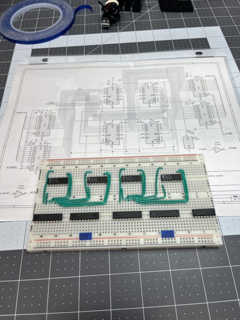
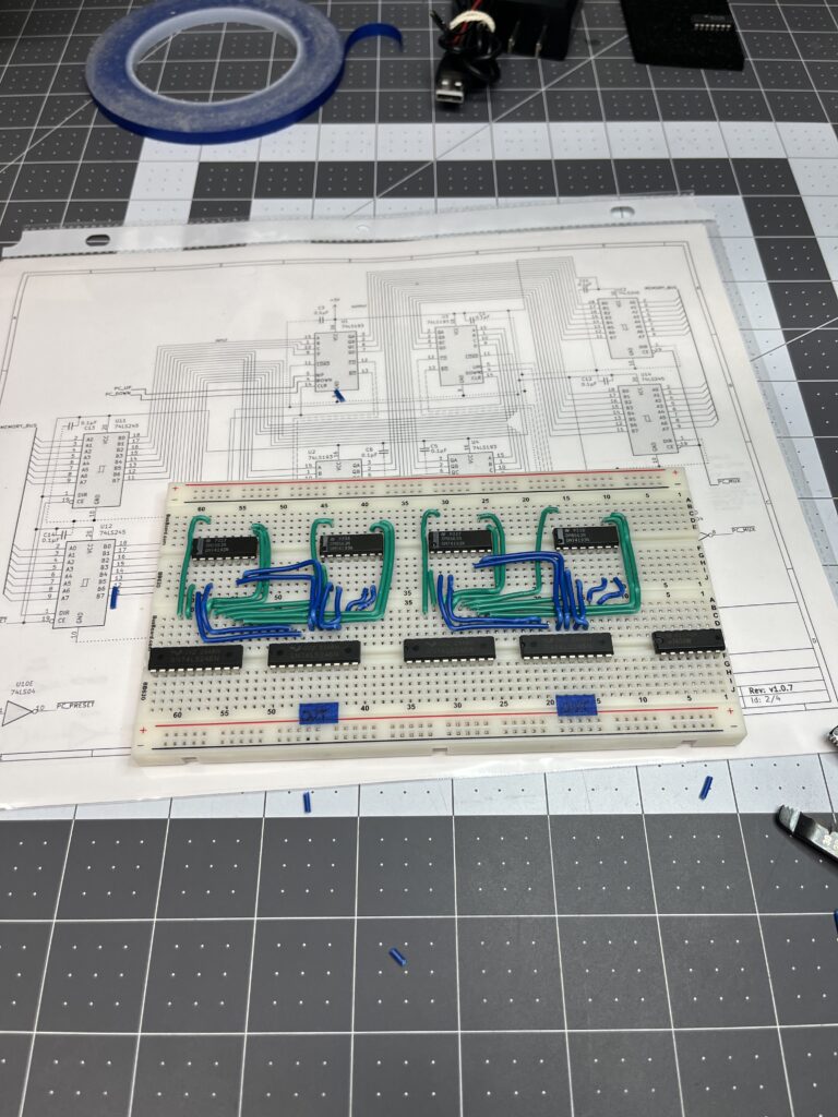
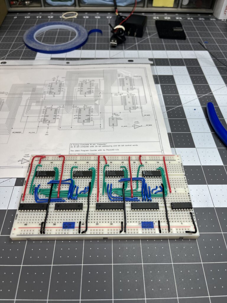
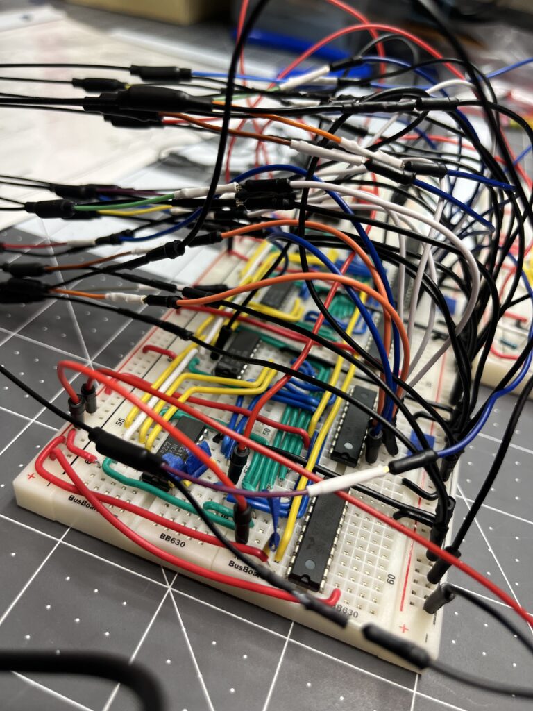
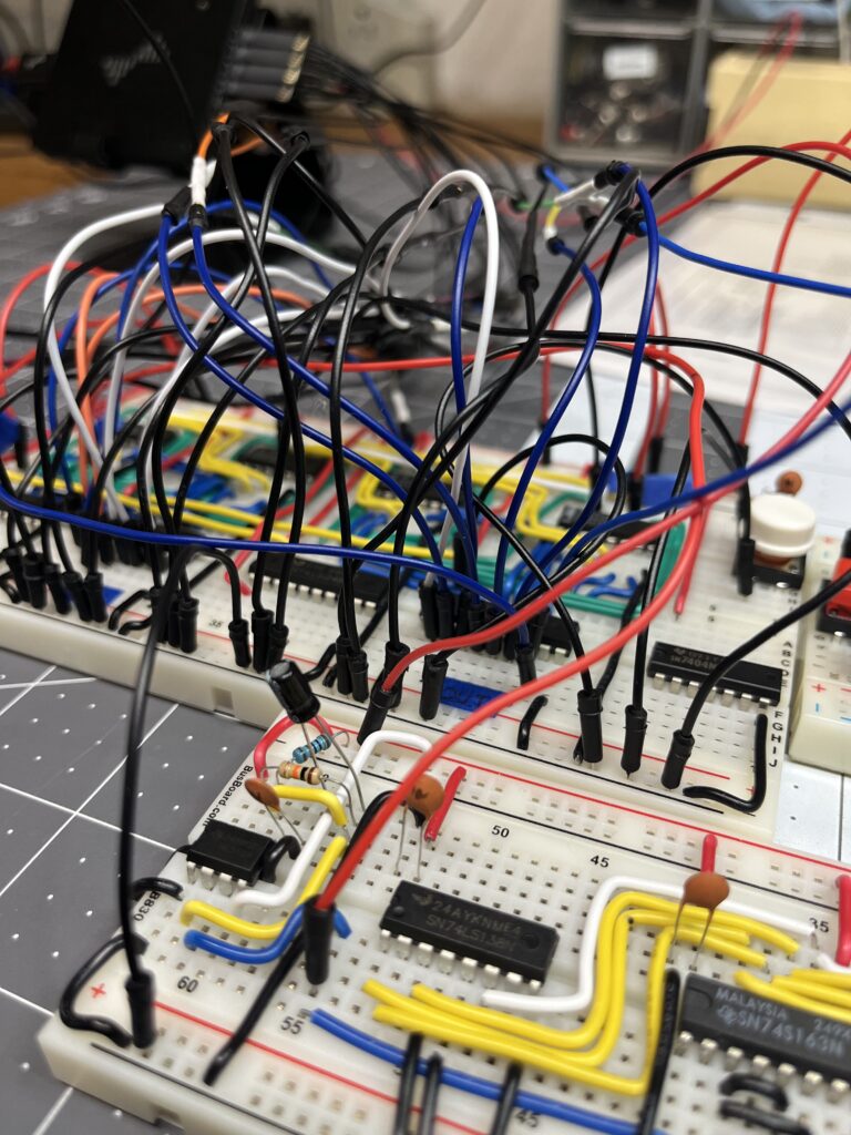
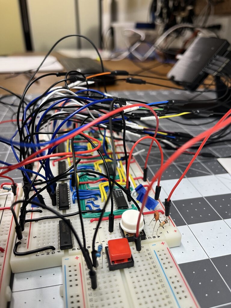
Construction Strategy and Pattern Recognition
Wiring Complexity Management
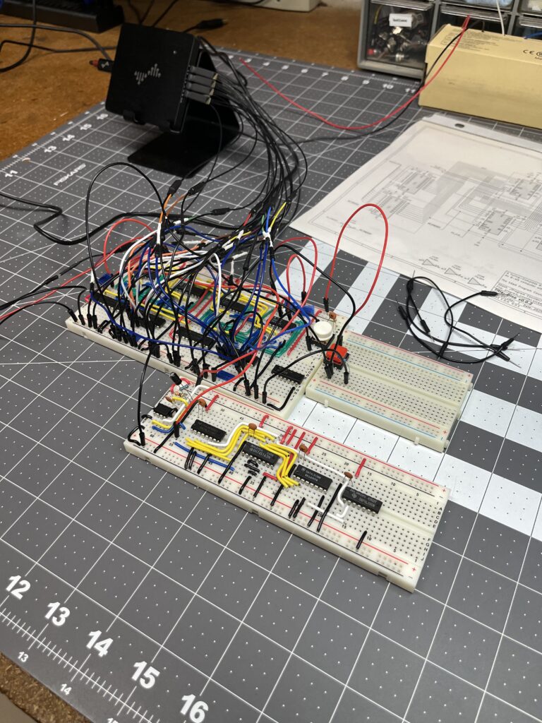
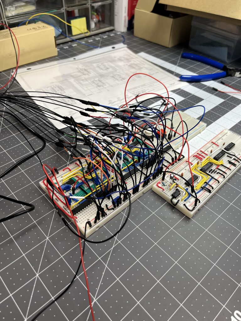
The 16-bit bus architecture demanded strategic construction planning beyond typical breadboard assembly:
- Dupont Jumper Pre-Fitting: Temporary connections identified potential wire routing conflicts before permanent installation
- Component Placement Optimization: Alternating input and output transceivers created natural wiring symmetries
- Pattern-Based Routing: Systematic cascade connections reduced complexity through visual consistency
Engineering Discovery
The construction process revealed how thoughtful component arrangement transforms chaotic wiring into organized patterns. Alternating transceiver placement created identical routing for all cascade connections, turning potential complexity into systematic regularity.
The result resembled engineered artwork – clean, predictable wire patterns that facilitated both construction and debugging.
Validation Results and System Integration
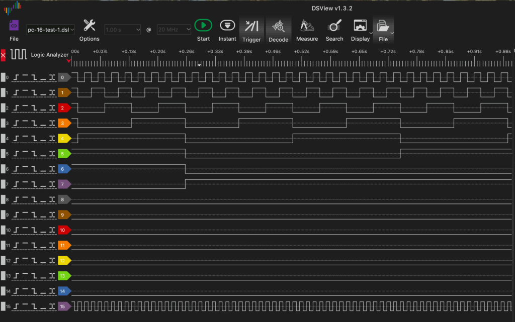
Logic Analyzer Verification
Complete 16-bit bus monitoring provided comprehensive visibility into counter operations:
- Immediate Success: All functionality operational on first power-up attempt
- Clean Transitions: No timing glitches or signal integrity issues observed
- Proper Cascading: Carry and borrow signals propagating correctly across all stages
Timing Dependency Resolution
Testing revealed critical insights about cascade signal timing requirements:
- Manual Control Limitations: Hand-operated up/down controls provided insufficient pulse width for cascade operations
- 555 Timer Integration: 60Hz clock delivered proper timing characteristics for ~BO/~CO signals
- Engineering Insight: Cascade functionality depends on clock pulse duration, not merely edge timing
Preset Capability Confirmation
Address loading validation completed the testing sequence:
- MSB Testing Strategy: Preset testing focused on high-order bits for immediate visual confirmation
- Construction Error Discovery: Input transceivers inadvertently hardwired during assembly process
- Rapid Resolution: Single connection correction restored full preset functionality
Engineering Significance and System Foundation
Complexity Management Success
The PC implementation validated key embedded development principles:
- Schematic-Driven Development: KiCAD circuit design prevented construction errors and enabled strategic component placement
- Systematic Validation: Pre-construction testing framework eliminated debugging uncertainty
- Methodical Assembly: Disciplined wiring approach prevented the chaos typical of complex breadboard circuits
Architectural Foundation Establishment
Successful PC operation provides the addressing infrastructure for complete CPU functionality:
- Instruction Sequencing: Reliable program advancement enables systematic instruction execution cycles
- Address Space Access: 16-bit capability provides substantial memory addressing range
- Control Word Integration: PC_MUX and PC_PRESET signals interface cleanly with established timing architecture
Methodology Validation
This milestone demonstrated how systematic engineering practices produce reliable results on complex multi-chip coordination problems. The combination of thorough design analysis, strategic testing protocols, and disciplined construction yielded first-attempt success on challenging timing-dependent hardware.
Development Trajectory: T0/T1 Decoder Implementation
The proven Program Counter establishes reliable address generation for the next critical phase:
- Universal Instruction Fetch: T0/T1 timing states will coordinate ROM-to-IR data movement
- Address Matrix Formation: Instruction Register output combined with ring counter states for control word indexing
- Bootstrap Sequence Architecture: Initial fetch capability enabling instruction execution without manual startup
The PC success provides engineering confidence for tackling the address formation complexity ahead.
Core Engineering Principle: Complex embedded systems achieve reliability through systematic subsystem validation before integration attempts. The Program Counter milestone exemplifies how disciplined analysis, careful construction, and comprehensive testing enable first-try success on demanding multi-chip timing coordination challenges.
The discrete logic computer advances toward complete computational capability through proven engineering methodology.