The Data Storage and Retrieval System
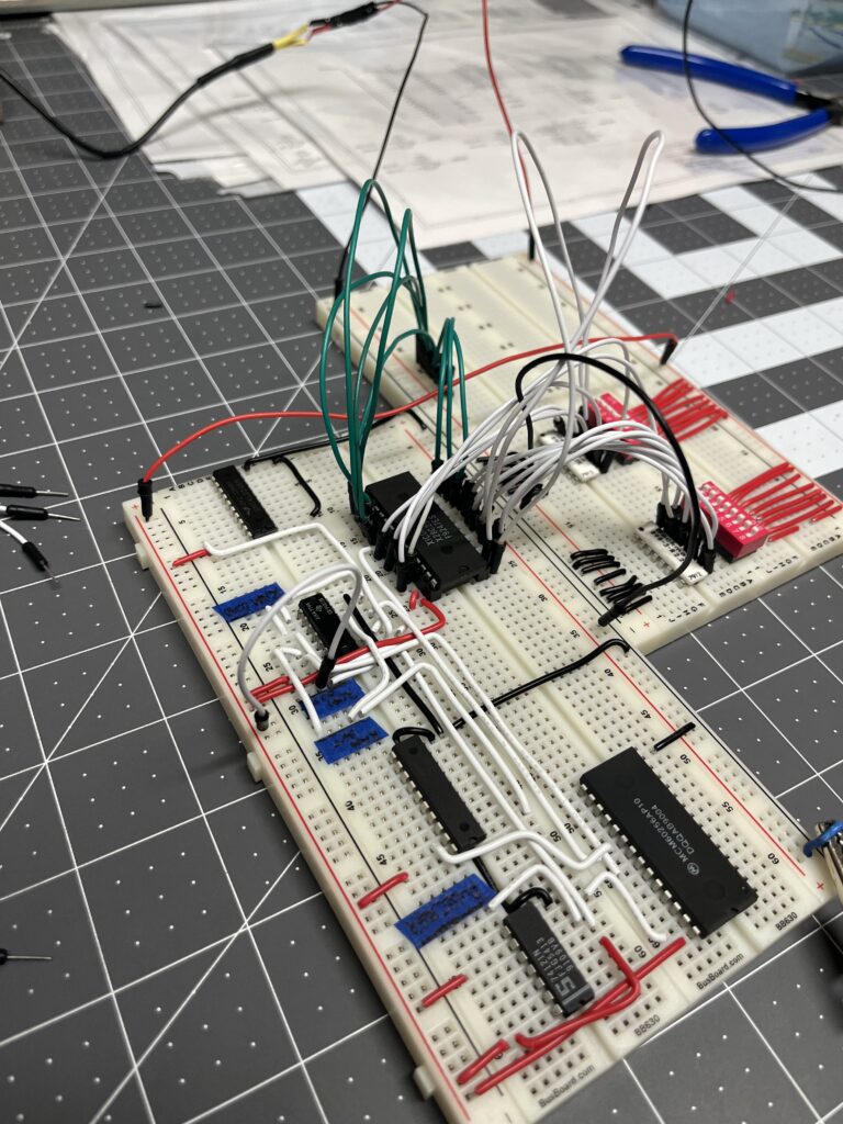
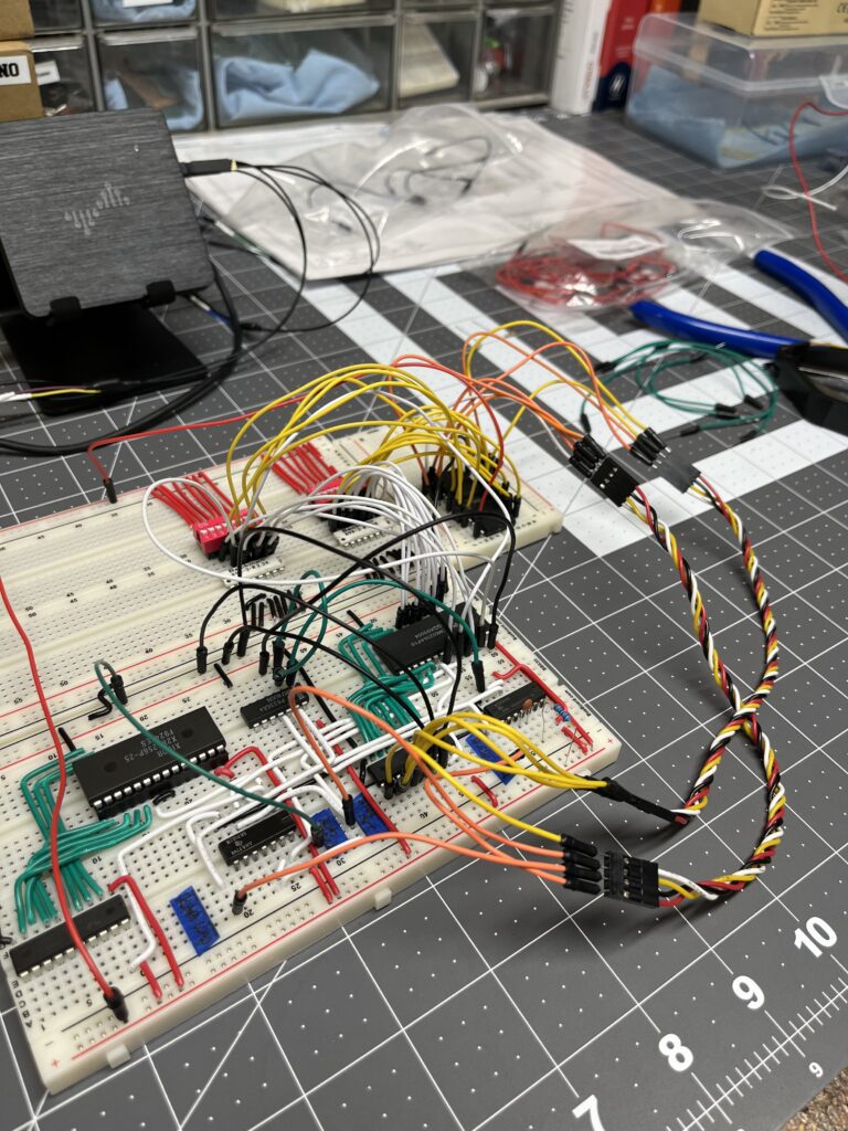
With the Microcode Decoder operational and generating control words, the next critical subsystem was the Memory Module. This module represents the CPU’s primary storage architecture — both the Program ROM containing instructions and the SRAM providing working memory. The Memory Module bridges the address bus to the data bus, orchestrating read and write operations under control of the microcode signals.
The implementation demanded meticulous attention to bit ordering, timing constraints, and bus arbitration. As with my other previous builds, this module required multiple schematic revisions to achieve deterministic operation.
Architectural Overview
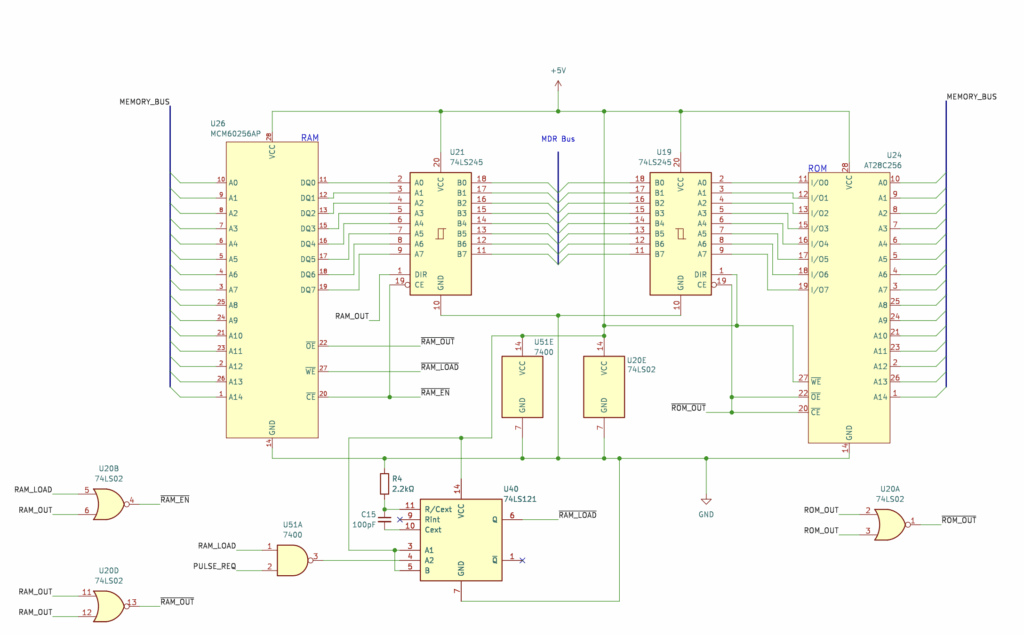
The Memory Module integrates:
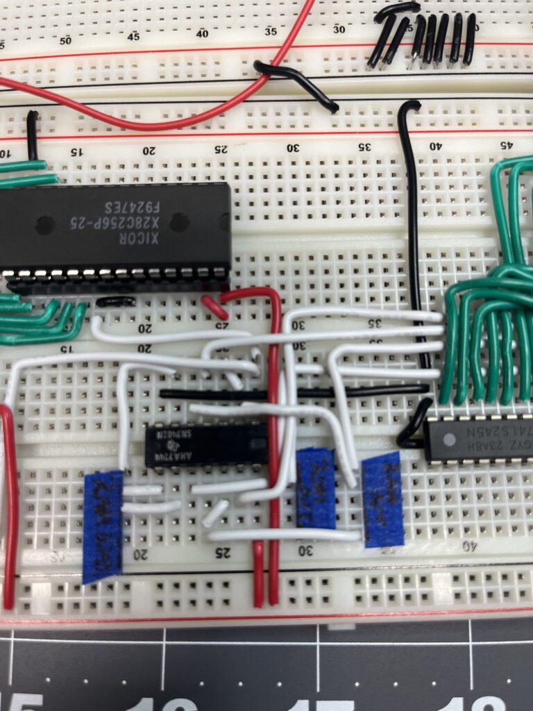
- AT28C256 EEPROM: 32KB Program ROM containing instruction sequences
- MCM60256 SRAM: 32KB RAM for data storage and manipulation
- 74LS245 Bus Transceivers: Bidirectional buffers preventing bus contention
- 74LS121 Monostable Multivibrator: Precision pulse generator for SRAM write timing
- 16-bit Address Bus: Shared addressing for both ROM and RAM
- 8-bit Data Bus: Common data pathway with LED monitoring
Bus Architecture and Arbitration
The original design specified 74LS244 unidirectional buffers for ROM output. However, the 74LS245 bidirectional transceiver proved superior even for unidirectional operation, providing consistent pinout and better drive characteristics.
Critical Discovery: I/O7 on both RAM and ROM chips represented the LSB, not the MSB as initially assumed. This revelation required rewiring the entire data bus interface to maintain consistent bit ordering across all modules. The discovery emerged during test rig construction when binary patterns didn’t match expected values.
Bus Control Strategy:
- ROM ‘245: DIR tied for output-only operation, OE controlled by ROM_OUT signal
- RAM ‘245: DIR controlled by RAM_LOAD/RAM_OUT for bidirectional operation
- Only one transceiver enabled at any time, preventing bus contention
The SRAM Write Timing Challenge
Initial attempts to write SRAM using clock phase levels failed consistently. Investigation revealed that the MCM60256 SRAM requires an edge transition on its WE (Write Enable) pin to latch data, not a sustained level.
Solution: Precision Pulse Generation
The 74LS121 monostable multivibrator generates a 600ns active-low pulse:
- Triggered simultaneously with other control signals
- Provides setup time for data bus stabilization
- Creates clean falling edge for SRAM write operation
- Returns high before next clock phase
RC Timing Calculation
The 74LS121 pulse width calculation:
t_pulse = 0.7 × R × C
600ns = 0.7 × 10kΩ × C
C = 86pF (100pF selected for margin)
Implementation Note: Both A1 and B inputs required pull-up to VCC for reliable triggering. Initial attempts to use PULSE_REQ directly on the B input created indeterminate behavior.
Control Signal Architecture
The Memory Module responds to four control bits from the Microcode Decoder:
| Signal | Function | Source |
|---|---|---|
| ROM_OUT | Enable ROM data onto bus | Bank 2, Code 001 |
| RAM_OUT | Enable RAM data onto bus | Bank 2, Code 010 |
| RAM_LOAD | Write bus data to RAM | Bank 2, Code 011 |
| PULSE_REQ | Trigger 121 for write pulse | Bit 12 |
Test Infrastructure Development
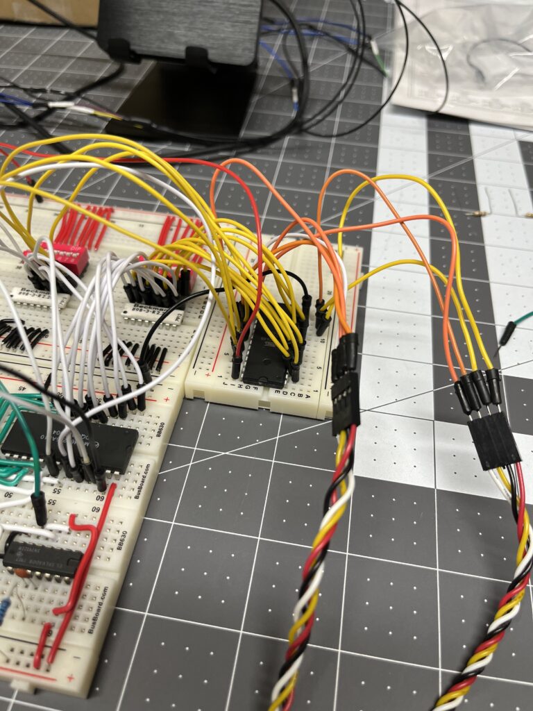
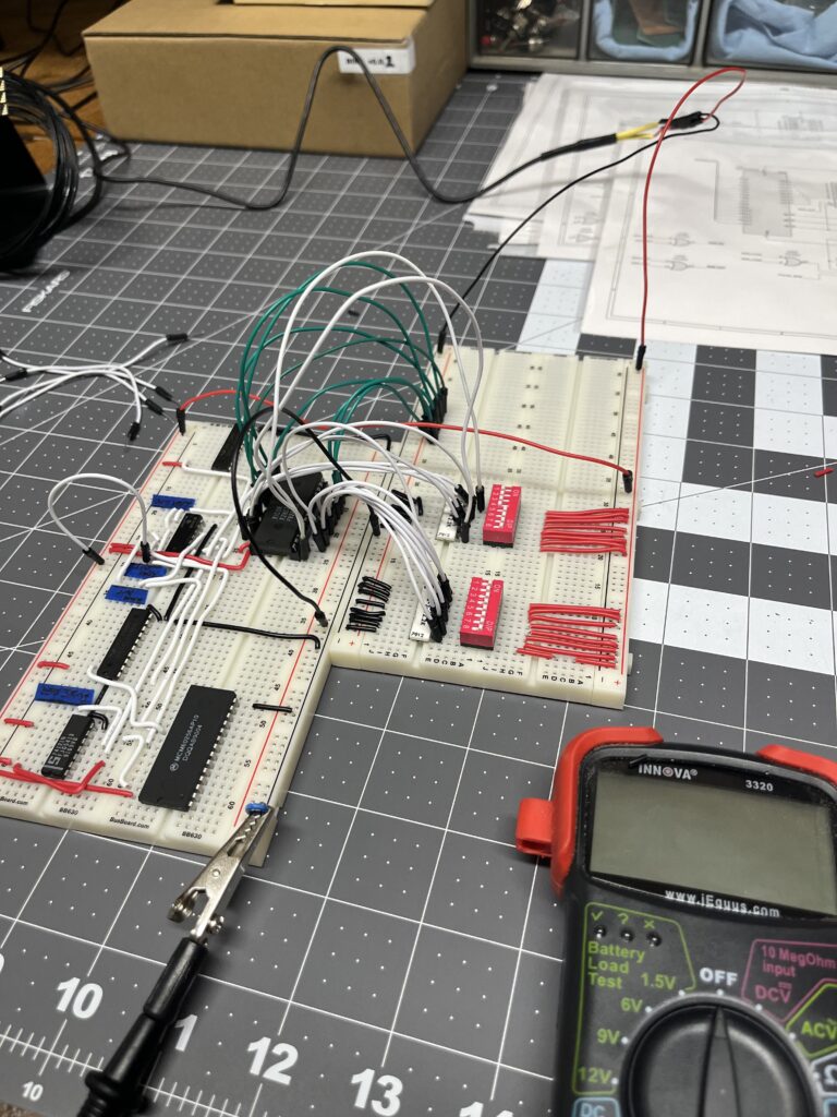
Testing required sophisticated input and output monitoring:
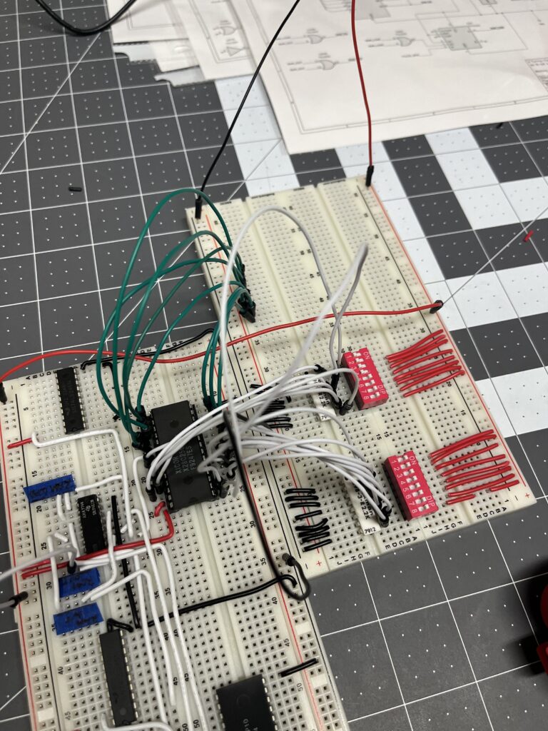
Input Test Rig
- 2 × 8-position DIP switches for manual address entry
- Beckman 3.3kΩ resistor arrays for switch pull-down
- Direct connection to 16-bit address bus
Output Monitoring
- 8 LEDs displaying current data bus state
- 220Ω current-limiting resistors
- Visual confirmation of read/write operations
Test Methodology and Validation
Dual Test Program Architecture
Testing the Memory Module required two distinct C programs to validate both ROM and RAM operations independently:
- Program ROM Test: Verification of EEPROM read operations
- SRAM Test Controller: Coordinated write/read validation with proper control signal timing
Program ROM Test Development
The first C program generated test patterns for the AT28C256 EEPROM:
// Key test addresses and values
eeprom[0x0000] = 0xAA;  // Alternating bit pattern
eeprom[0x0001] = 0x55;  // Inverse pattern
eeprom[0x1234] = 0x12;  // Address-based value
eeprom[0xABCD] = 0xCD;  // High address test
Test ROM Mini-Microcode Controller
The critical innovation was developing a dedicated Test ROM that acted as a miniature microcode controller specifically for SRAM testing. This second C program generated control word sequences that could:
- Write data patterns to the bus
- Assert RAM_LOAD simultaneously with PULSE_REQ
- Coordinate RAM_OUT for read verification
- Maintain proper control signal timing relationships
This Test ROM approach better reflected actual system integration where the Microcode Decoder would generate all control signals simultaneously, rather than manual switch manipulation that could introduce timing skew.
Systematic Test Sequence
- ROM_OUT Validation
- Set DIP switches to test address
- Assert ROM_OUT via Test ROM control pattern
- Verify LED pattern matches burned EEPROM data
- Confirmed: ROM data successfully appears on bus
- PULSE_REQ Verification
- Test ROM generates PULSE_REQ signal
- Monitor 74LS121 output with oscilloscope
- Confirm 600ns pulse width with clean edges
- Confirmed: Pulse generation operates within specifications
- RAM_LOAD Operation (via Test ROM)
- Test ROM places data pattern on bus
- Simultaneously asserts RAM_LOAD and PULSE_REQ
- All control bits loaded in parallel, mimicking actual microcode operation
- Confirmed: Data latched into SRAM as expected
- RAM_OUT Verification
- Test ROM switches to read mode
- Asserts RAM_OUT for previously written address
- Compare bus output to written value
- Confirmed: Complete write-read cycle functional
The mini-microcode Test ROM validated that simultaneous control signal assertion worked correctly — a critical requirement for integration with the actual Microcode Decoder module.
Debugging Discoveries
Address Confusion Resolution
Initial testing showed data corruption — writing to one address but reading incorrect values from another. Root cause: attempting to share the 16-bit address generator between test ROM reads and SRAM operations.
Solution: Separate address generation for each test phase. This “classic case of trying to move too fast” reinforced the importance of methodical, isolated testing.
Trigger Logic Refinement
Original NOR gate configuration for 74LS121 triggering proved unreliable. Multiple schematic revisions led to a clean NAND gate implementation that provided deterministic pulse generation.
Schematic Evolution
The Memory Module underwent three major schematic revisions:
- Initial design with 74LS244 buffers and level-triggered writes
- Migration to 74LS245 transceivers with pulse generator addition
- Final refinement of trigger logic and pull-up configurations
Each revision reflected lessons learned during hardware testing, demonstrating the iterative nature of discrete logic design.
Engineering Insights
The Memory Module implementation reinforced several critical principles:
- Bit Ordering Discipline: Consistent LSB/MSB conventions across all modules prevents cascading debug sessions
- Edge vs. Level Triggering: Understanding component timing requirements before design prevents fundamental architectural errors
- Isolated Testing: Attempting to share test infrastructure between different operations creates confusion and masks real issues
- RC Circuit Fundamentals: The 0.7 factor in 74LS121 timing calculations represents practical engineering constants that must be respected
Milestone Confirmation
The Memory Module is fully operational, providing:
- Reliable ROM instruction fetches
- Deterministic SRAM read/write cycles
- Clean bus arbitration without contention
- Validated timing margins for all operations
Next Phase: Memory Data Register
With the Memory Module complete, the next implementation is the Memory Data Register (MDR) — the critical buffer between memory operations and the CPU’s internal registers. The MDR will provide the temporary storage necessary for complex addressing modes and multi-cycle operations.
The systematic progression continues: each module building upon validated foundations, methodically constructing a complete discrete logic computer from fundamental components.
