The Challenge that Started Everything
After mastering bare-metal C programming and wrestling with the RP2040’s ROM assumptions in my OTA bootloader project, a fundamental question emerged: what happens below the microcontroller abstraction layer? Modern MCUs hide extraordinary complexity behind simple APIs – but understanding computation from first principles required going deeper.
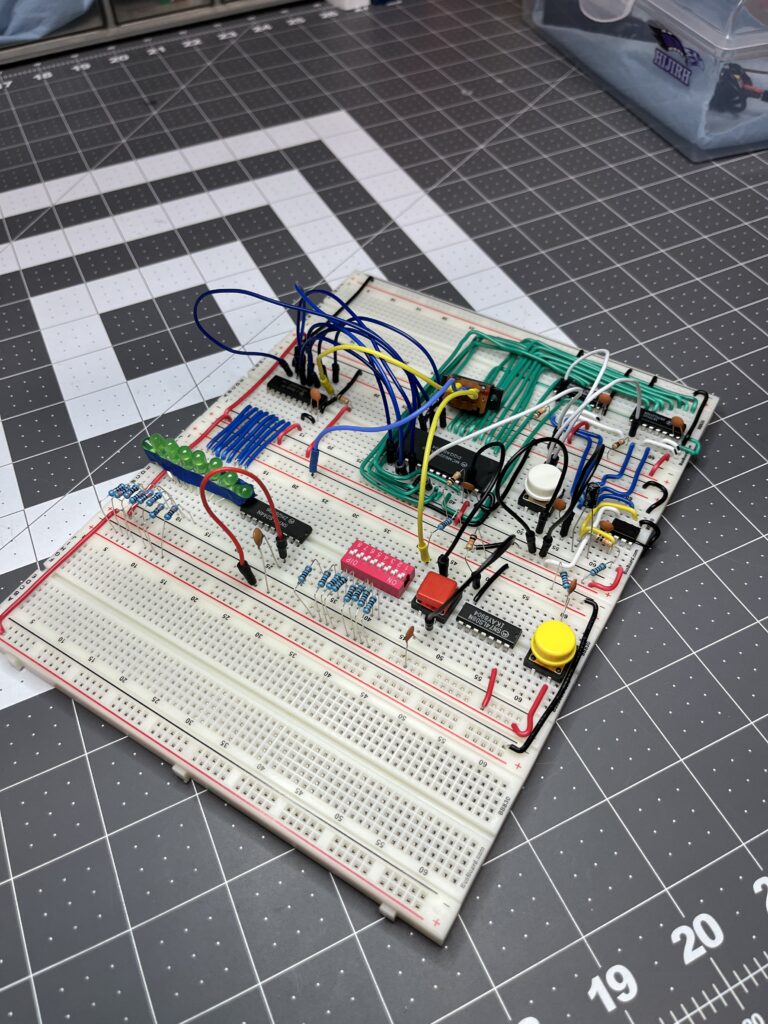
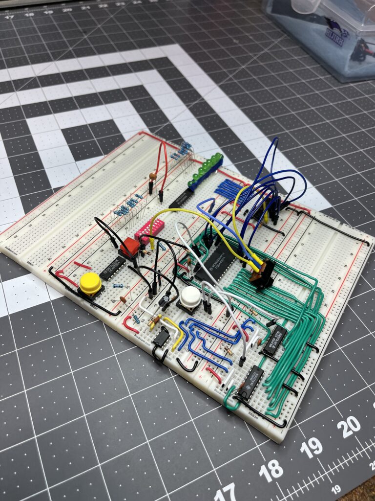
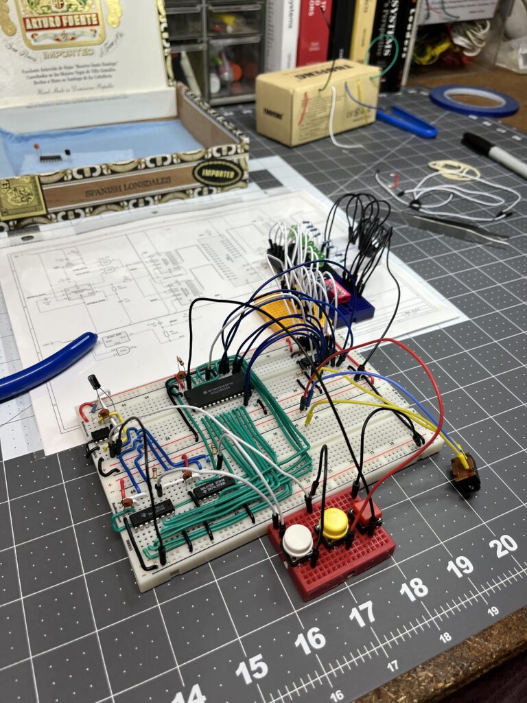
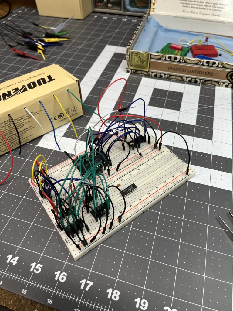
The DINO CPU project represents an attempt to build computational capability using only discrete logic components – counters, memory, ALU chips, and control logic. No microcontrollers, no firmware, just the fundamental building blocks that make computation possible.
What I Set Out to Build
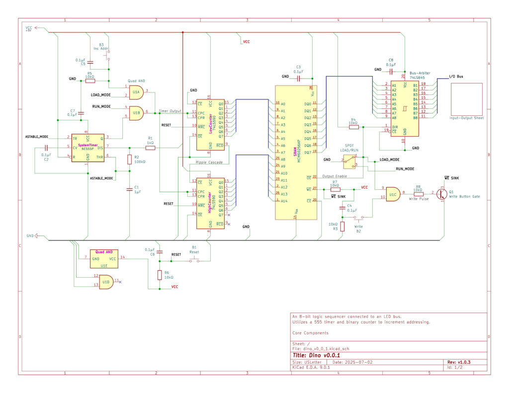
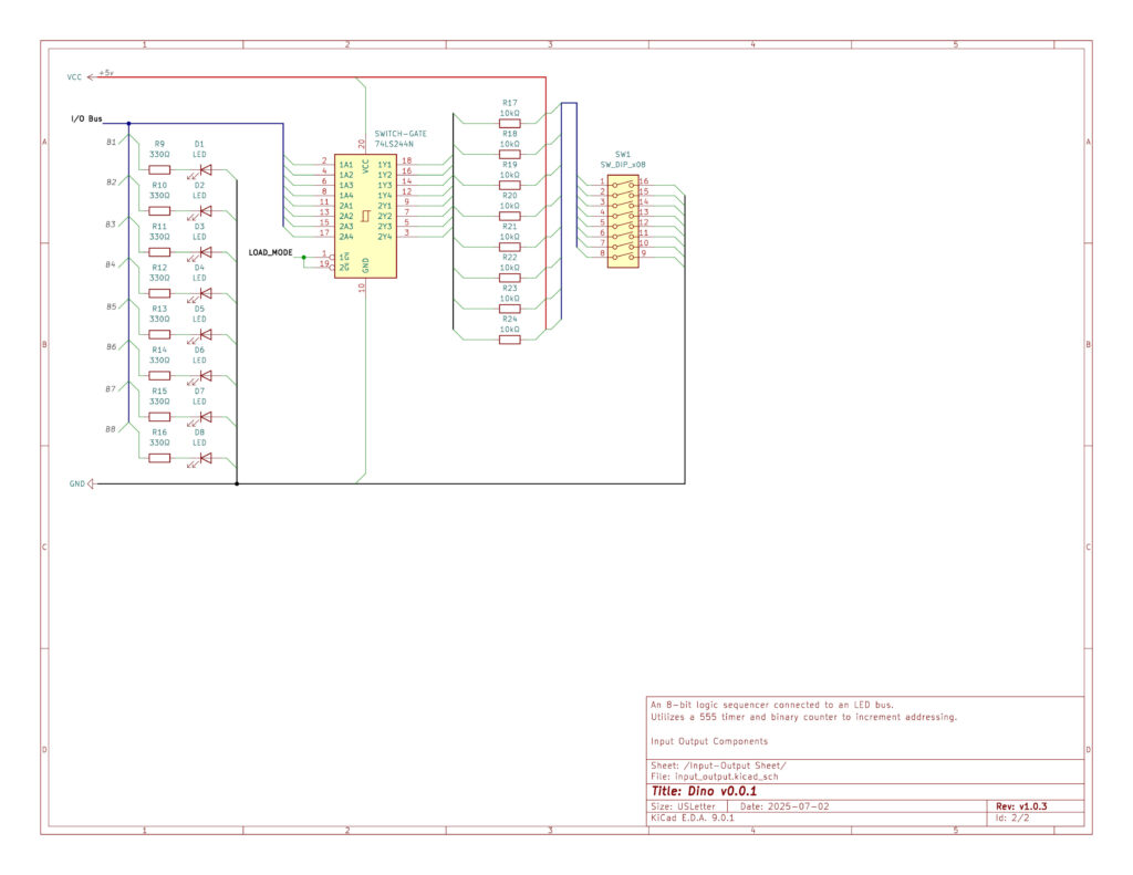
System Architecture:
- 8-bit data path with 16-bit addressing capability
- Von Neumann architecture (shared instruction/data memory)
- 32KB addressable memory space
- Real-world application: Thermistor temperature monitoring with digital display and analog output
Component Foundation:
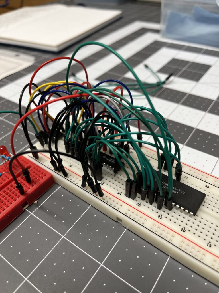
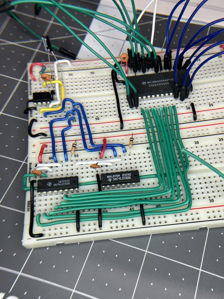
- Memory: MCM60256AP-10 32KB SRAM for program storage
- Program Counter: SN74LS590N 8-bit counters chained for 16-bit addressing
- Bus Control: 74LS645N octal transceiver for bus arbitration
- Clock Generation: 555 timer providing controlled system timing
- ALU: 74F382N 8-bit arithmetic logic unit for computation
The goal wasn’t just to blink LEDs – it was to create a system capable of reading temperature sensors, performing calculations, and driving both digital displays and analog outputs.
The Engineering Reality
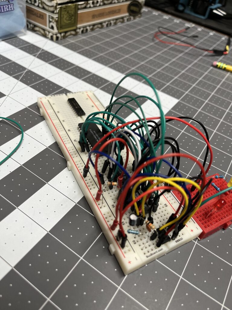
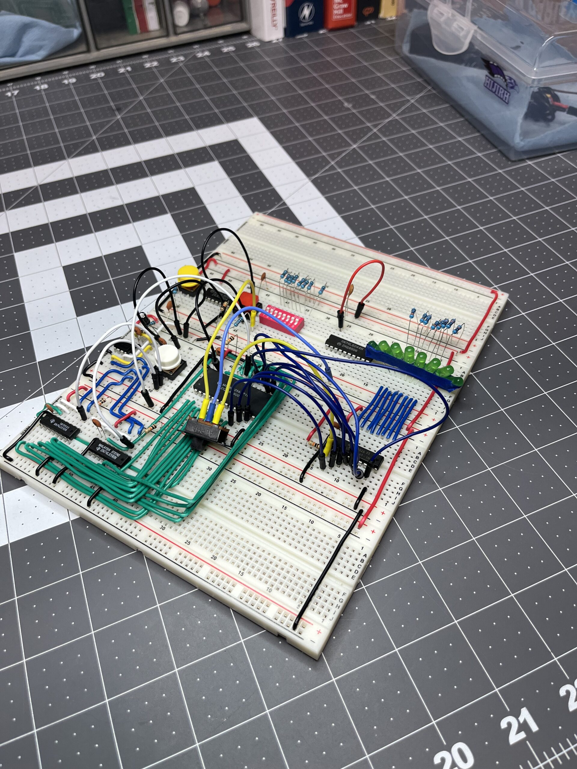
Phase 1: The Deceptively Simple Beginning
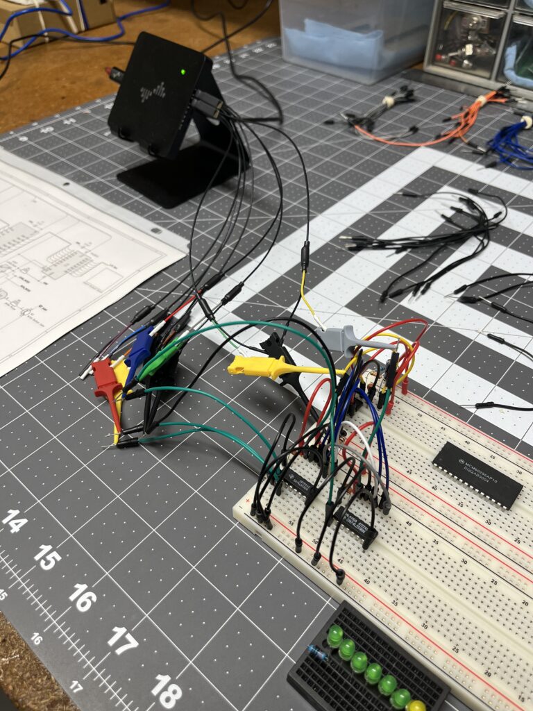
The initial approach seemed straightforward: build a CPU-free sequencer that could step through memory addresses and display stored patterns on LEDs. Two modes: LOAD (program data via DIP switches) and RUN (execute stored sequence).
Early Success Indicators:
- Clean 16-bit address generation from chained counters
- Successful SRAM read/write operations
- Mode switching between programming and execution
- LED patterns displaying correctly
The basic sequencer worked exactly as designed. I could manually program LED chase sequences, store them in SRAM, and watch them execute reliably. This initial success masked the complexity that lay ahead.
The Control Logic Revelation
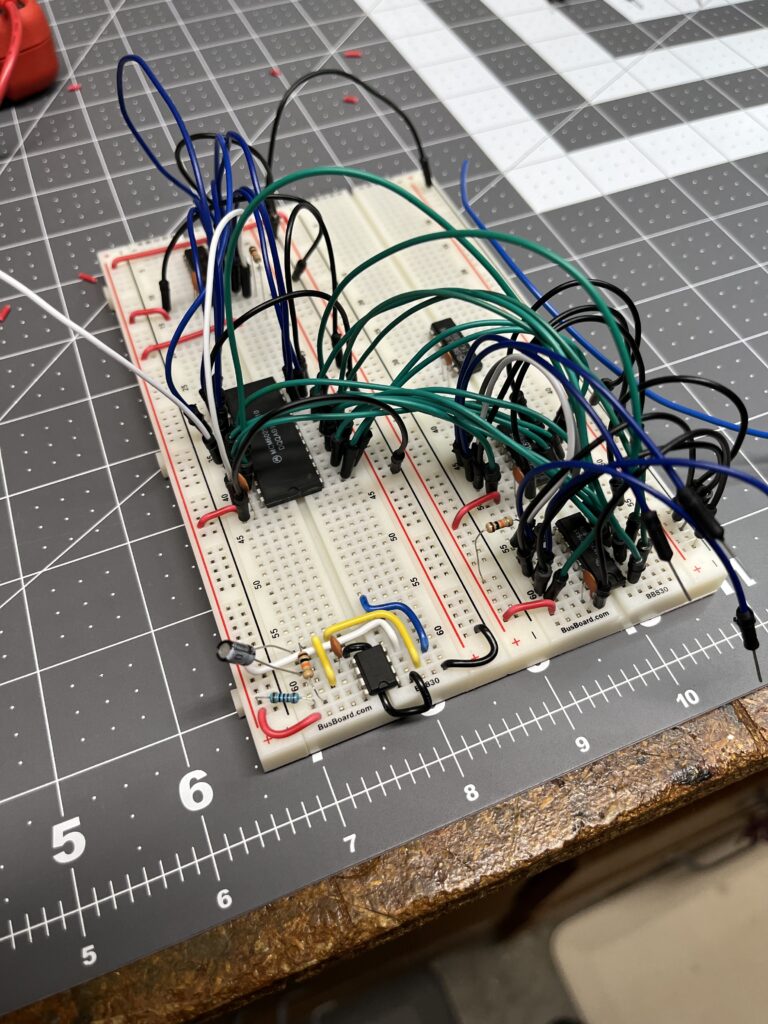
What initially appeared as simple mode switching (LOAD vs. RUN) revealed itself as a fundamental architectural challenge. The moment I attempted to coordinate multiple bus devices – DIP switches, SRAM, and LED displays – the limitations of my approach became clear.
Bus Arbitration Issues: DIP switches provided weak logic levels insufficient for reliable SRAM write operations. The 74LS645 bus transceiver required precise timing coordination that simple SPDT switches couldn’t provide. Signal integrity problems emerged immediately.
Interdependency Testing: Components couldn’t be validated independently due to circular dependencies between memory interface and mode control logic. The SRAM operation depended on proper bus control, but bus control verification required working SRAM access.
Control Logic Complexity: What I had designed as simple combinational logic – AND gates and switches – proved inadequate for coordinating multiple bus devices with different timing requirements.
The Architecture Limitation
The fundamental issue wasn’t component selection or circuit construction – it was control system architecture. Real computers require systematic control word generation, not ad-hoc switching logic.
Control Word Requirements:
- Coordinated timing for instruction fetch, decode, and execute cycles
- Bus arbitration preventing multiple drivers
- Sequence management for multi-cycle operations
- Error handling and state recovery
My initial design using SPDT switches and basic gates couldn’t generate the sophisticated control signals required for reliable computer operation.
The Strategic Pivot
Reference Architecture Investigation
Rather than abandoning the project, I shifted to studying proven methodologies. Albert Paul Malvino’s “Digital Computer Electronics” and the SAP (Simple As Possible) computer architecture provided the systematic approach my initial design lacked.
Key Insights from SAP-1:
- Control logic requires state machines, not simple combinational circuits
- Instruction cycles need multiple clock phases with coordinated timing
- Bus control demands systematic enable/disable sequencing
- Memory operations require setup and hold time management
Engineering Maturity Recognition
The project revealed a critical gap in my engineering approach. I had been pattern-matching from successful circuits without understanding the underlying control theory that makes computers reliable.
Methodology Evolution:
- From ad-hoc circuit assembly to systematic control design
- From hoping circuits work to proving they meet timing requirements
- From debugging failures to preventing them through proper design
- From component-focused to system-focused engineering
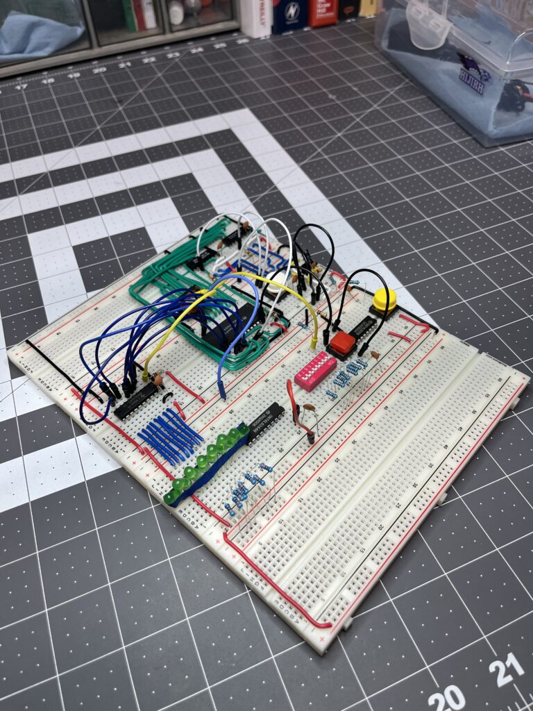
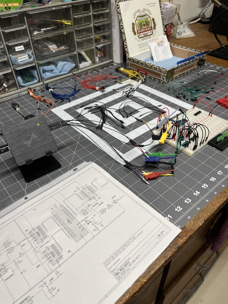
Current Status and Lessons Learned
Preserved Working Elements
The investigation wasn’t a complete loss. Several subsystems function correctly and provide a foundation for systematic reconstruction:
- Validated 16-bit program counter implementation with proper chaining
- Functional SRAM read/write interface with verified timing margins
- Working power distribution and signal conditioning circuits
- Proven component selection appropriate for the target application
Knowledge Gained
Signal Integrity Requirements: Real-world digital logic demands attention to current sourcing, logic levels, and bus loading effects that breadboard prototypes often hide.
Control System Architecture: Computer control logic requires systematic state machine design, not intuitive switching circuits.
Timing Analysis Methodology: Reliable digital systems need verified setup/hold times, not just “fast enough” clock speeds.
Modular Design Discipline: Complex systems require independently testable subsystems with well-defined interfaces.
The Engineering Insight
This project exemplifies how the most valuable learning emerges from systematic analysis of apparent failures. What began as frustration with non-working circuits became comprehensive understanding of computer architecture principles.
The investigation process – methodical debugging, component-level testing, and willingness to study fundamental theory when initial approaches failed – proved more valuable than any working computer would have been initially.
Future Direction
Systematic Reconstruction Plan
The project continues with enhanced methodology, combining original architectural goals with proven control system design principles:
Immediate Objectives:
- Document current system state and verified component functionality
- Study SAP-1 control logic principles and timing methodology
- Design modular test interfaces for independent subsystem validation
- Implement systematic control word generation using proven techniques
- Rebuild with emphasis on testable, verifiable operation
Long-term Vision:
- Complete 8-bit computer capable of thermistor monitoring application
- Systematic documentation enabling others to understand and replicate
- Foundation for exploring advanced computer architecture concepts
- Platform for investigating computation principles from silicon upward
Engineering Philosophy Evolution
The DINO project transformed my understanding of embedded systems engineering. Previous projects succeeded despite gaps in fundamental knowledge. This project exposed those gaps and provided the motivation to fill them systematically.
Key Realization: Understanding why systems work matters more than just making them work. The debugging methodology, control theory insights, and systematic design principles gained here enable confident approaches to any digital logic challenge.
Project Significance
DINO represents more than an attempt to build a computer – it embodies the engineering discipline of understanding computational systems from first principles. The systematic analysis of control logic requirements, timing constraints, and system architecture provides knowledge applicable far beyond discrete logic projects.
The project continues as a long-term educational investment, combining practical engineering with fundamental computer science concepts. Understanding computation at the silicon level informs every higher-level embedded project that follows.