How I tried, failed and dug deeper to get OTA proper without a library on the PicoW RP2040
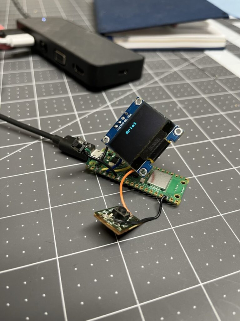
After the success of PicoBook, implementing Over-The-Air firmware updates seemed like the logical next step. Every deployed embedded device needs remote update capability, and the RP2040’s dual-core architecture with ample flash storage appeared well-suited for a dual-partition bootloader system.
The goal was straightforward: build a minimal OTA system without external libraries, using only the Pico SDK. Firmware A (bootloader) would download new firmware images over Wi-Fi, write them to a reserved flash partition, and jump cleanly to the new code. Standard embedded practice, with existing reference implementations to guide the approach.
What started as a weekend project became a three-week deep dive into RP2040 boot architecture, ARM Cortex-M initialization sequences, and the hidden assumptions buried within seemingly simple SDK functions. The project “failed” in that no working OTA system emerged, but succeeded in exposing fundamental knowledge gaps that would reshape my entire approach to embedded development.
This documentation captures both the technical investigation process and the engineering insights that made every subsequent project possible.
Initial Architecture & Approach
The design followed standard embedded OTA patterns: a dual-partition system with clearly defined memory regions and responsibilities.
Flash Layout:
- Bootloader (Slot A):
0x10000000–0x10064000(400KB) - Boot Flag Region:
0x10064000–0x10065000(4KB) - Application Firmware (Slot B):
0x10065000onwards (512KB+)
Operational Flow:
- Bootloader checks boot flag and validates existing firmware
- If update required, downloads new firmware via Wi-Fi to Slot B
- Verifies download integrity and sets boot flag
- Performs manual jump to new firmware’s reset vector
Jump Implementation Strategy:
The critical transition from bootloader to application required setting up the ARM Cortex-M execution environment manually:
uint32_t sp = *(uint32_t*)(app_base);    // Load stack pointer
uint32_t entry = *(uint32_t*)(app_base + 4); // Load reset handler
__asm volatile("msr msp, %0" :: "r"(sp));    // Set main stack pointer
*(volatile uint32_t*)0xE000ED08 = app_base;  // Update vector table offset
((void (*)())entry)(); // Jump to application
This approach worked perfectly in theory and matched successful reference implementations. The bootloader compiled cleanly, established Wi-Fi connections, and successfully downloaded firmware binaries to the correct flash addresses.
Early Success Indicators:
- Clean compilation with proper linker script separation
- Successful Wi-Fi connection and HTTP downloads
- Verified flash writes at target addresses
- Valid vector table generation in downloaded firmware
The system appeared functional until the critical moment: jumping to the new firmware consistently triggered immediate HardFaults.
The Hard Fault Investigation
Initial Symptoms: Every jump to downloaded firmware triggered immediate HardFaults, despite valid vector tables and successful flash writes.
GDB Trace Analysis:
gdb
#3  __aeabi_double_init ()
#2  0x00000000 in ?? ()
#1  <signal handler>
#0  isr_hardfault ()
The crash occurred during __aeabi_double_init(), specifically on this line:
memcpy(&sd_table, rom_table_double, SF_TABLE_V2_SIZE);Key Discovery: rom_table_double pointed to 0x00000000 instead of valid ROM data.
Memory Inspection Revealed:
(uint16_t*)0x18=0x0000(should point to ROM function table)(uint16_t*)0x1C=0x0000(should point to float dispatch table)- These pointers are only initialized during cold boot by the RP2040 ROM
Root Cause: The Pico SDK assumes ROM-initialized state that doesn’t exist after manual firmware jumps. Cold boot initializes critical lookup tables; manual jumps bypass this entirely.
Solutions Attempted
Approach 1: ROM State Reconstruction – Based on reverse engineering the RP2040 boot sequence, I attempted to manually recreate the ROM’s initialization:
c
// Fake ROM boot environment before jump
(uint16_t)0x18 = 0x001D; // rom_func_lookup pointer
(uint16_t)0x1C = 0x024C; // rom_table_double pointer
((uint8_t)0x24A)[0] = 0x01; // Float table header ((uint8_t)0x24A)[1] = 0x40; // Table size (256 bytes)
Approach 2: AEABI Function Table Initialization – The crash revealed that aeabi_mem_funcs[] was never populated. Manual initialization:
c
extern void *__wrap_memcpy(void *, const void *, unsigned);
*(uint32_t*)(0x20000270 + 4) = (uint32_t)&__wrap_memcpy;
Approach 3: Link Register Safety – ARM functions expect valid return addresses in lr. Direct jumps leave it uninitialized:
c
// Trap value__asm volatile ("mov lr, %0" :: "r" (0xFFFFFFFF));

__attribute__((noreturn)) void (*app_entry)(void) = (void(*)(void))(reset_handler);
Approach 4: Complete Runtime Bootstrap – Manual .data and .bss section initialization for the target firmware:
c
memcpy(&data_start, &data_load_start, data_size);
memset(&bss_start, 0, bss_size);
Partial Success: Each approach solved specific crash symptoms but revealed deeper dependencies. The 256-byte SRAM5 region, ROM lookup tables, and SDK initialization sequences formed an interconnected web of assumptions.
The 256-Byte Discovery
Critical Breakthrough: While investigating SRAM usage, I discovered the RP2040’s 256-byte secret.
ROM Boot Sequence: The RP2040 ROM copies the first 256 bytes from flash (0x10000000) to SRAM5 (0x20040000), performs CRC verification, and executes it as the second-stage bootloader. This region remains accessible after boot.
Live Memory Experiment:
(gdb) x/64x 0x20040000 0x20040000: Valid structured code matching flash content
(gdb) set {unsigned int}0x20040000 = 0xdeadbeef
(gdb) x/8x 0x20040000 0x20040000: 0xdeadbeef # Memory is writable!Implications:
- The ROM doesn’t lock this region after boot
- SDK and firmware can read/write this memory
- It contains the actual executed bootloader code
- Could be used for persistent boot flags or metadata
Engineering Insight: This discovery revealed how little I understood about the RP2040’s actual boot process. The datasheet mentioned the 256-byte region, but experiencing it live through GDB – seeing writable executable code in RAM – made the boot architecture tangible.
Documentation Discipline: Each discovery was immediately documented with GDB commands, memory dumps, and hypothesis testing. This methodical approach became crucial as the investigation deepened.
Reality Check: The project was no longer about implementing OTA updates. It had become an archaeology expedition into embedded system assumptions.
Project Outcome & Learning Assessment
Technical Result: No functional OTA system delivered after three weeks of intensive development.
Engineering Value: Comprehensive understanding of RP2040 boot architecture, ARM Cortex-M initialization requirements, and embedded system dependency chains.
Critical Realization: The gap between “SDK-guided development” and “bare-metal systems engineering” was far wider than anticipated. High-level APIs hide essential knowledge required for reliability-critical embedded systems.
Knowledge Gaps Exposed:
- ARM EABI calling conventions and runtime requirements
- Memory section management (
.data,.bss,.vectors) - Linker script behavior and symbol resolution
- ROM-firmware interaction patterns
- Assembly-level debugging techniques
Methodology Validation: The systematic investigation approach – GDB traces, memory dumps, assembly analysis, datasheet correlation – proved essential for embedded debugging. Each tool revealed different aspects of the same complex problem.
Trajectory Impact: This project fundamentally changed my approach to embedded development. The “failure” exposed the necessity of understanding systems from silicon behavior upward, not just API usage downward.
Next Phase Catalyst: The investigation revealed that effective embedded engineering requires fluency in C, assembly, and hardware architecture. This directly motivated the transition to bare-metal development curriculum that followed.
Conclusion
This project exemplifies how the most valuable learning often emerges from apparent failures. What began as a straightforward OTA implementation became a masterclass in embedded systems architecture, revealing the intricate dependencies hidden beneath seemingly simple SDK functions.
The investigation process – systematic debugging, documentation discipline, and willingness to dig deeper when initial approaches failed – proved more valuable than any working bootloader would have been. Understanding why the RP2040 behaves as it does, rather than just how to make it work, became the foundation for every subsequent project’s success.
Key Takeaway: Embedded systems engineering requires understanding the full stack from silicon behavior to application logic. SDK abstractions are powerful tools, but they can’t substitute for fundamental knowledge when building reliability-critical systems.
Technical Legacy: The debugging methodology, memory management insights, and ARM architecture knowledge gained here directly enabled the bare-metal C work that followed. The “failed” OTA project became the prerequisite for every successful project afterward.
Return Intent
This project will be revisited. The investigation revealed exactly what’s required – manual ROM state reconstruction, runtime bootstrapping, and careful memory management. The bare-metal curriculum that followed built the prerequisite knowledge to implement these solutions correctly. When resumed, this will demonstrate how foundational understanding transforms impossible complexity into systematic engineering.
Engineering Philosophy: Sometimes the best projects are the ones that don’t work as intended but teach you everything you need to know for the next challenge.