Category: Projects

  • DINO CPU Project – Memory Module Implementation

    DINO CPU Project – Memory Module Implementation

    The Data Storage and Retrieval System

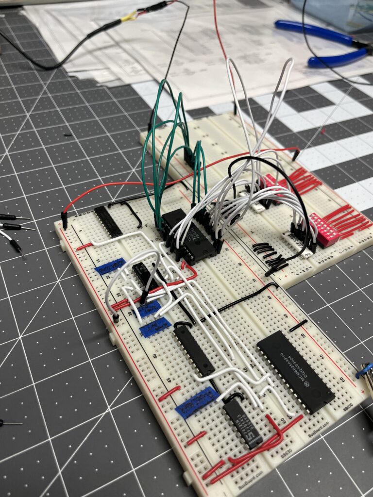
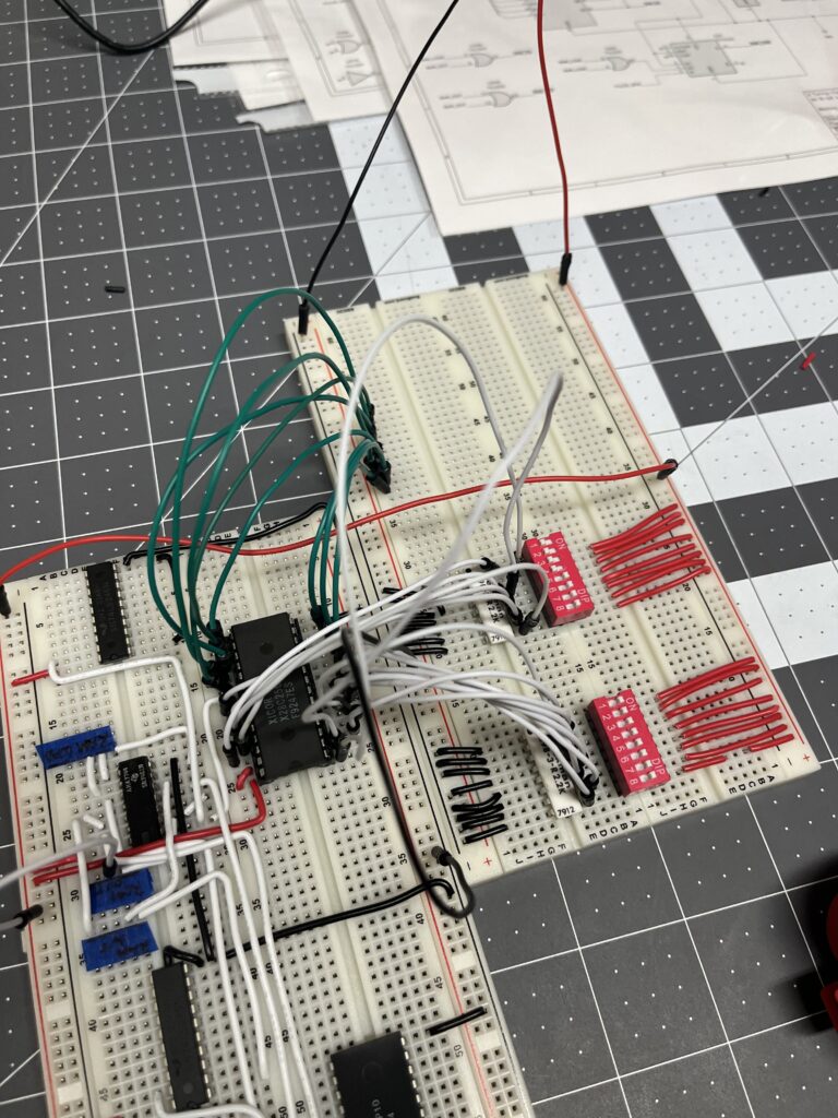
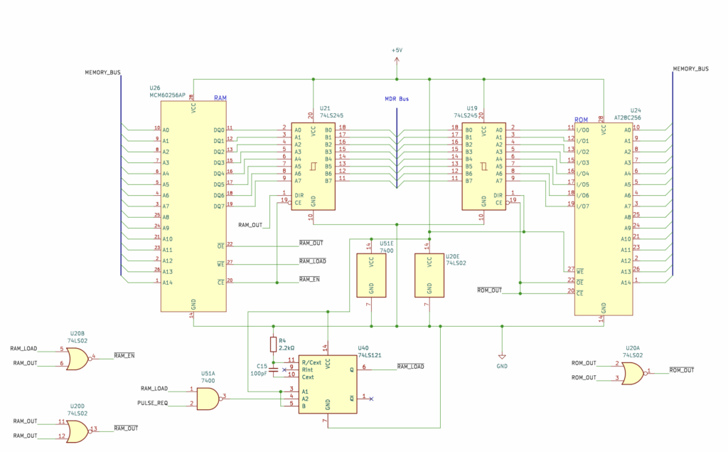
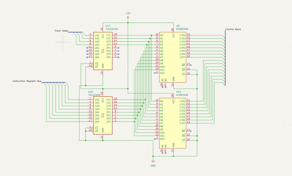
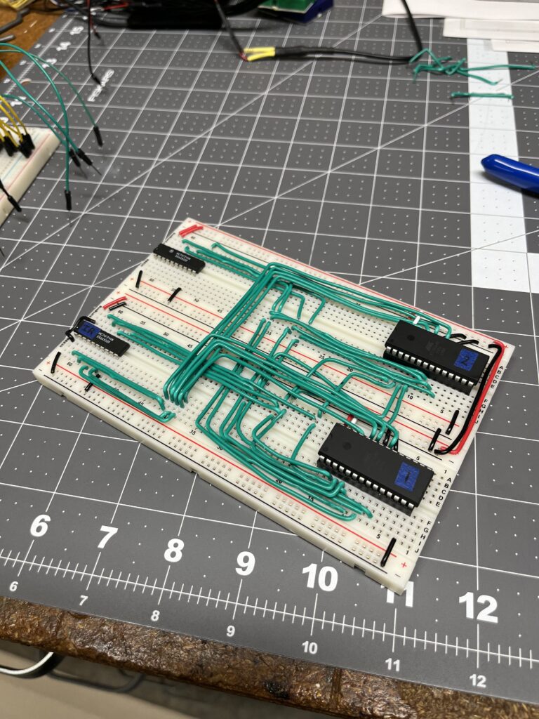
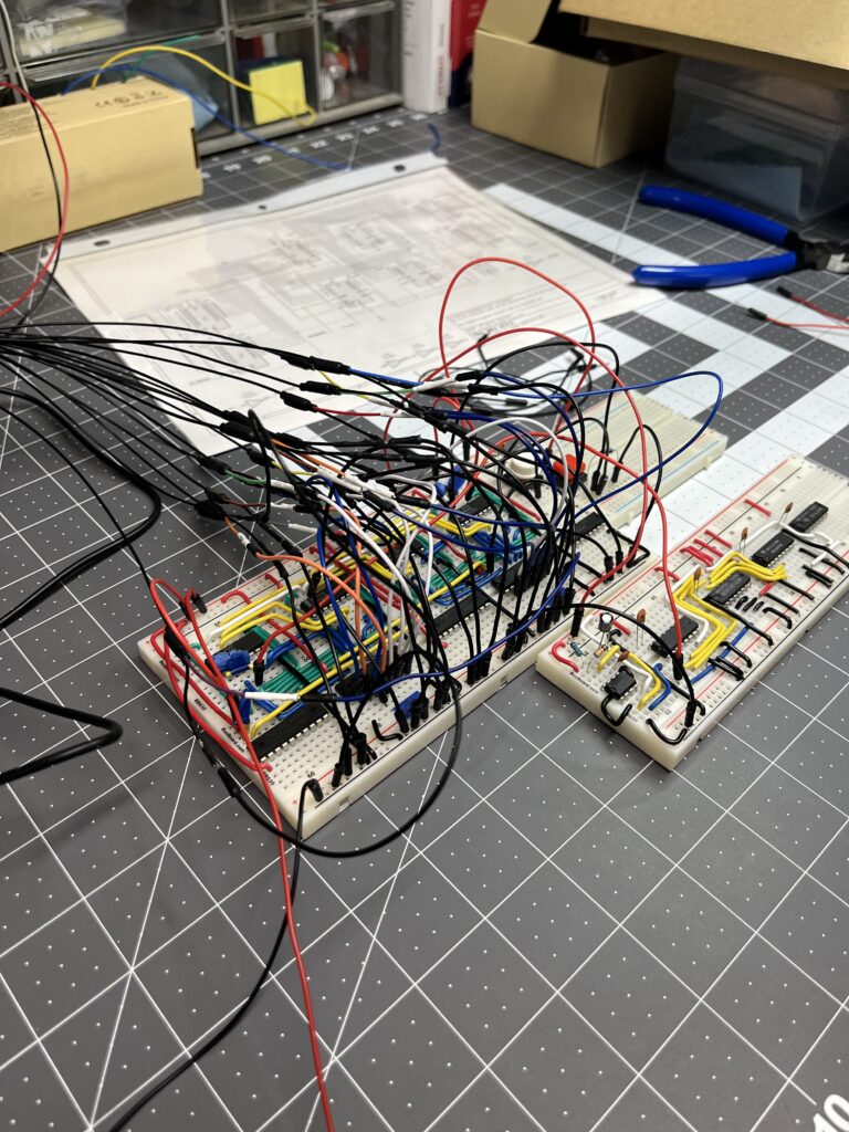
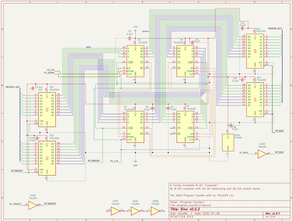
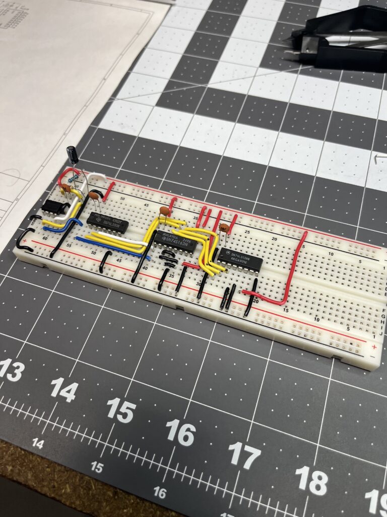
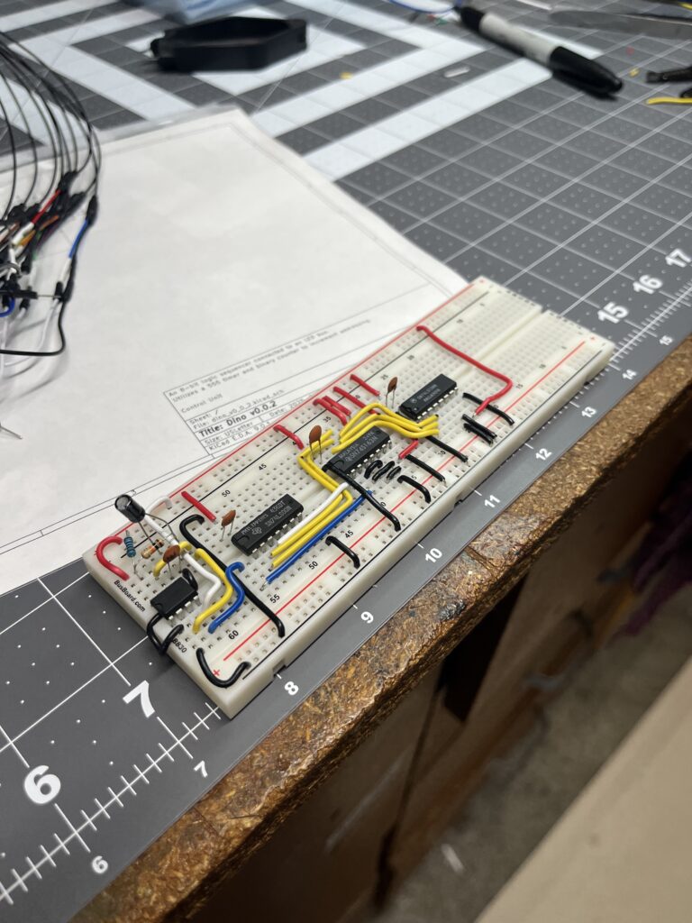
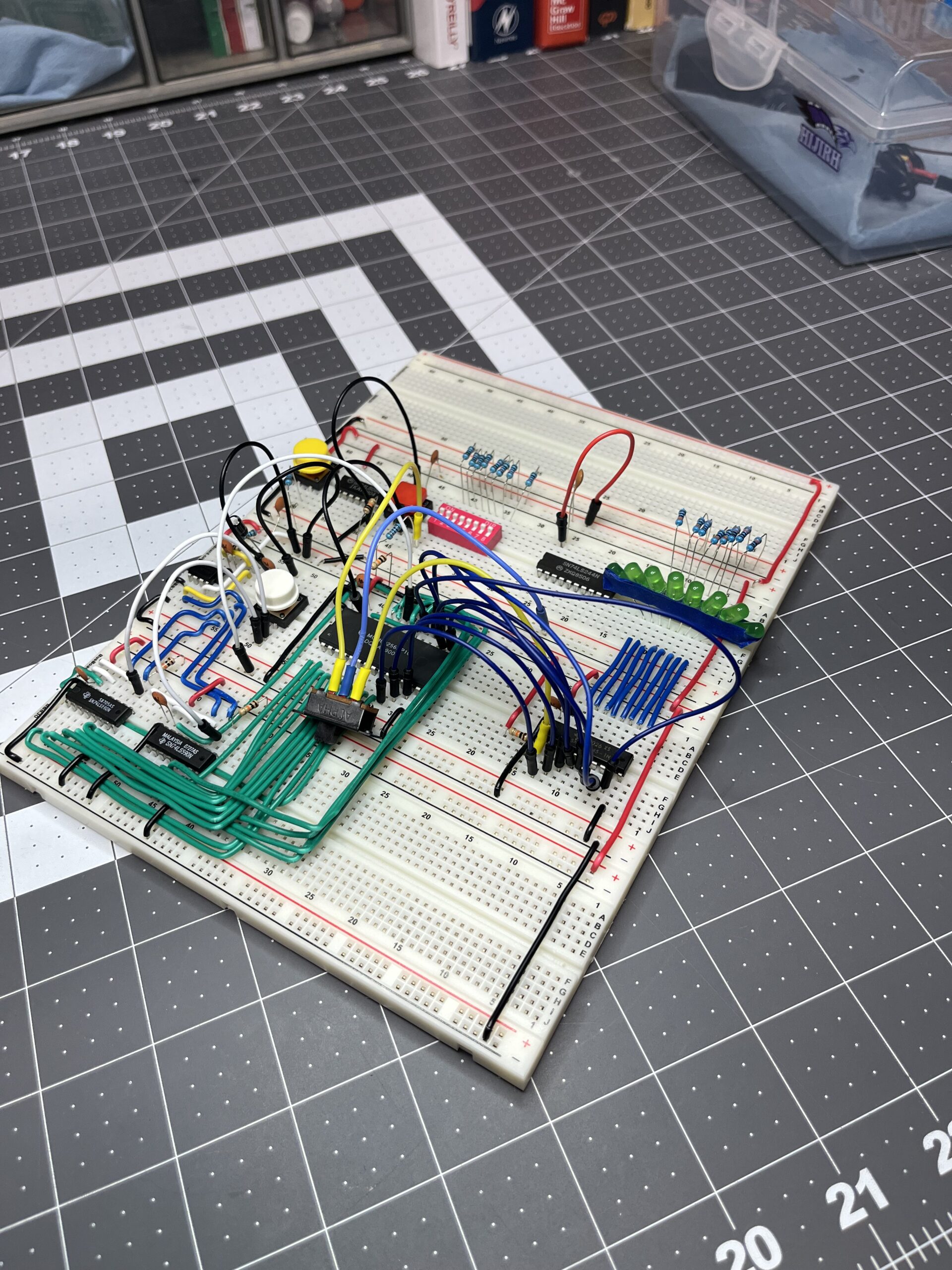
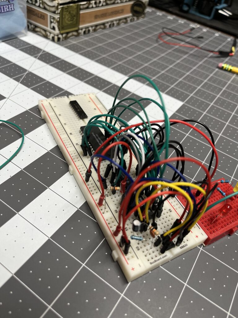
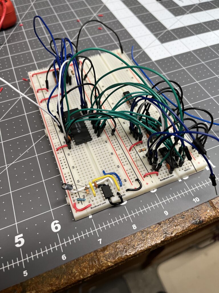
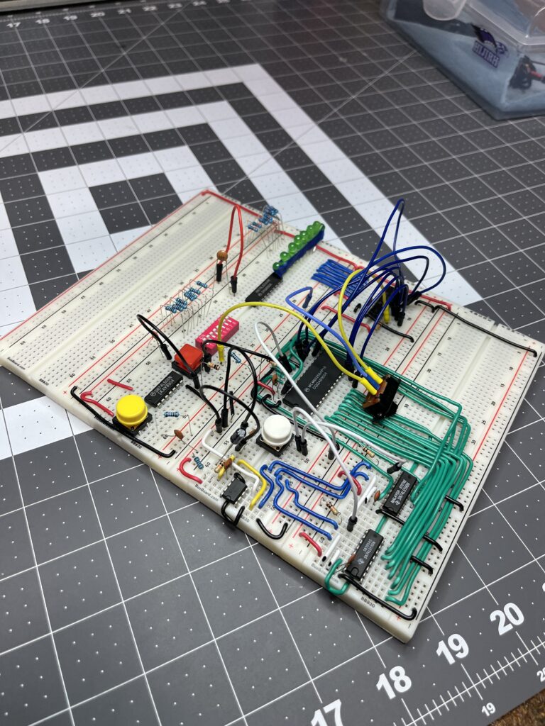
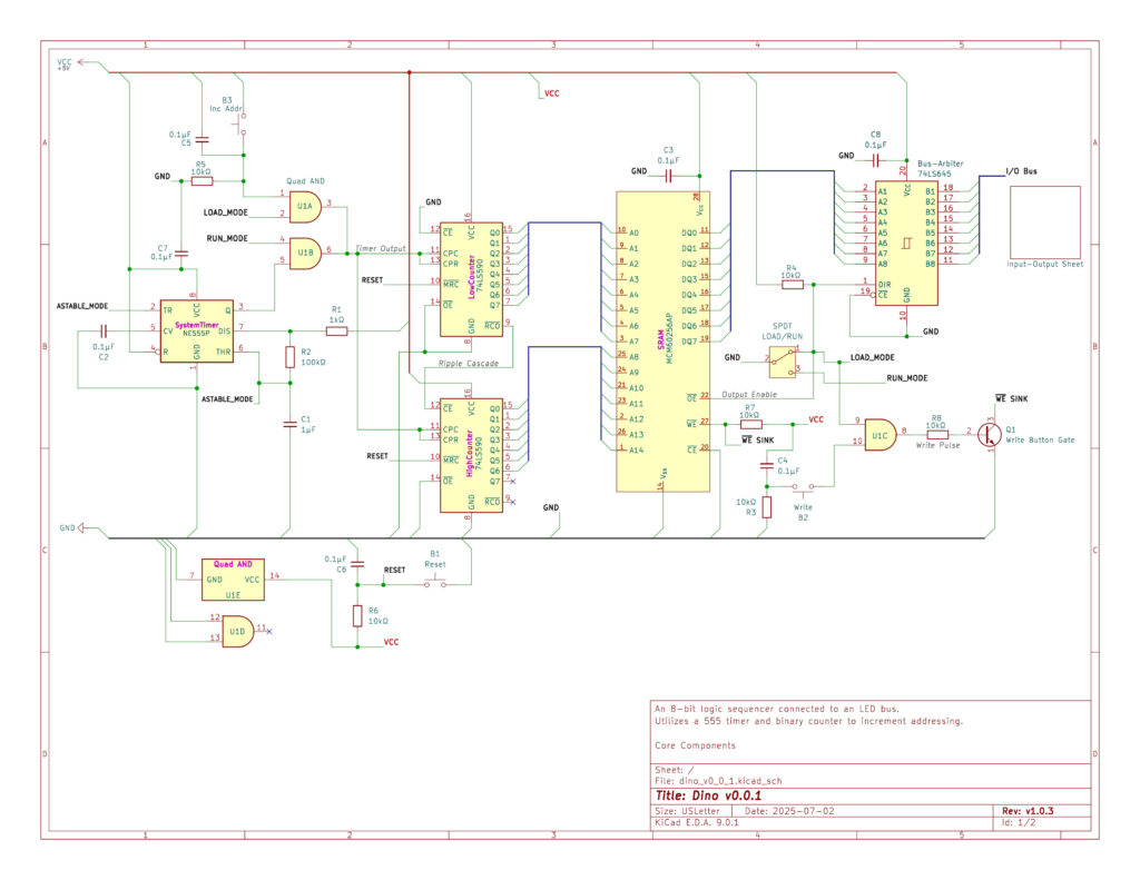
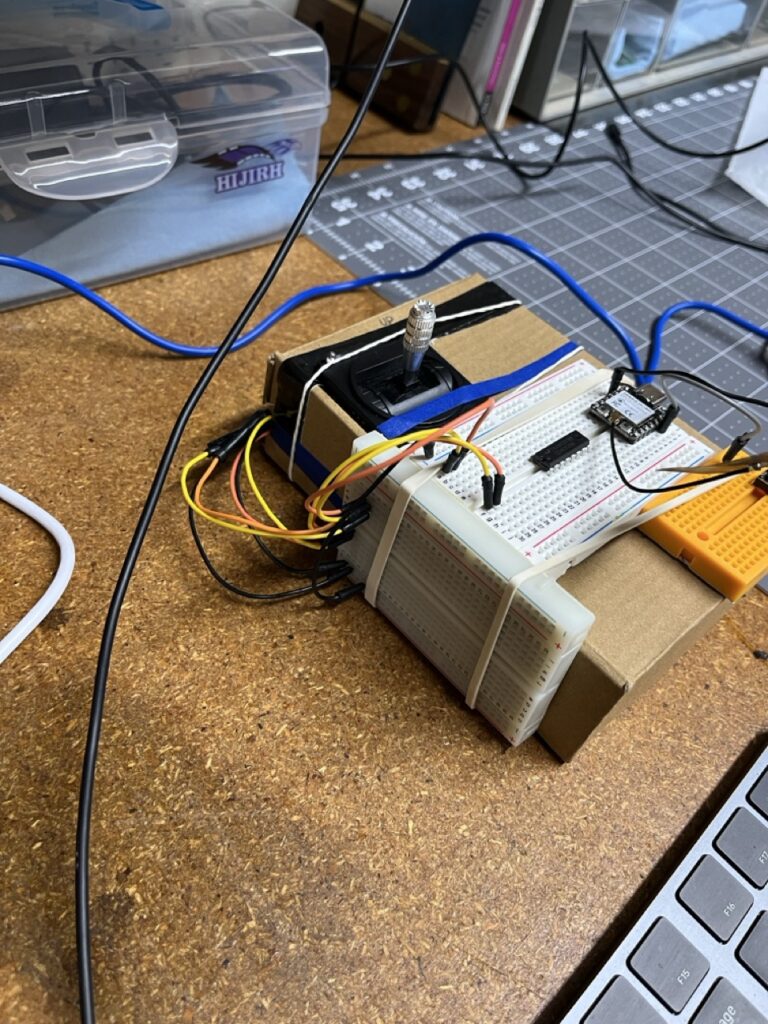
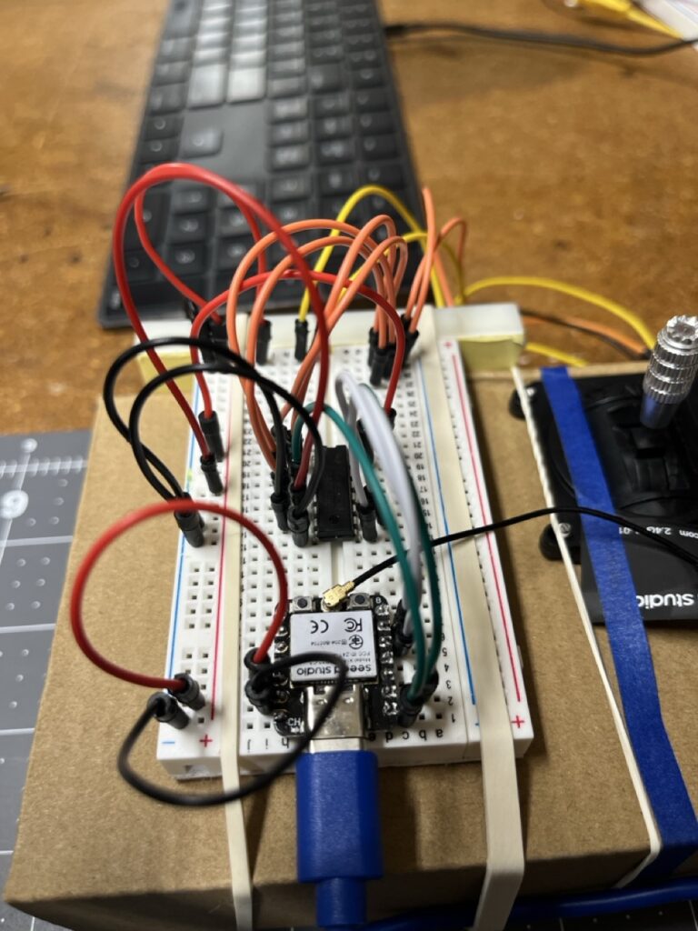
    With the Microcode Decoder operational and generating control words, the next critical subsystem was the Memory Module. This module represents the CPU’s primary storage architecture — both the Program ROM containing instructions and the SRAM providing working memory. The Memory Module bridges the address bus to the data bus, orchestrating read and write operations under control of the microcode signals.

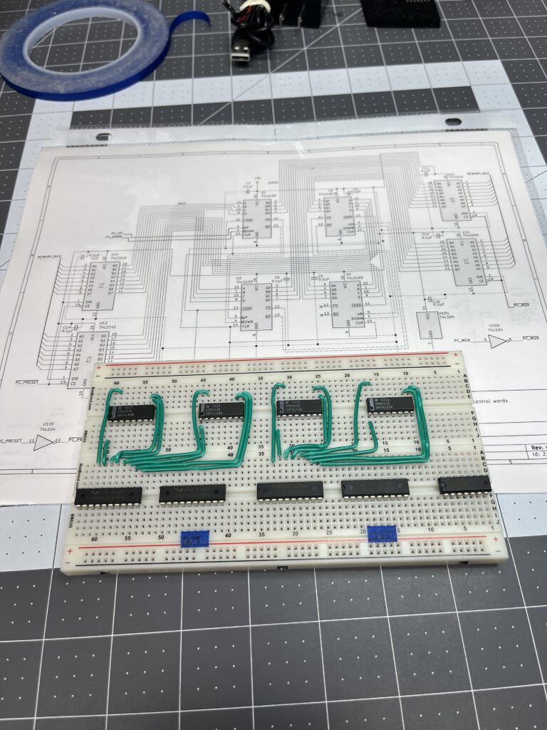
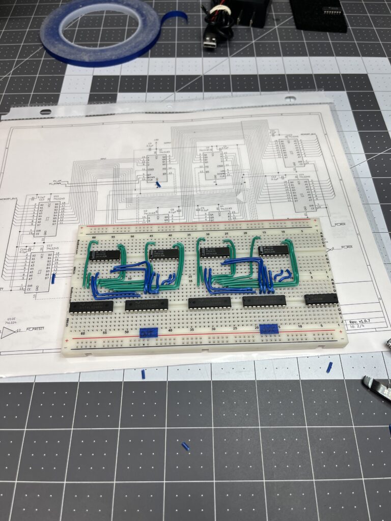
    The implementation demanded meticulous attention to bit ordering, timing constraints, and bus arbitration. As with my other previous builds, this module required multiple schematic revisions to achieve deterministic operation.

    Architectural Overview

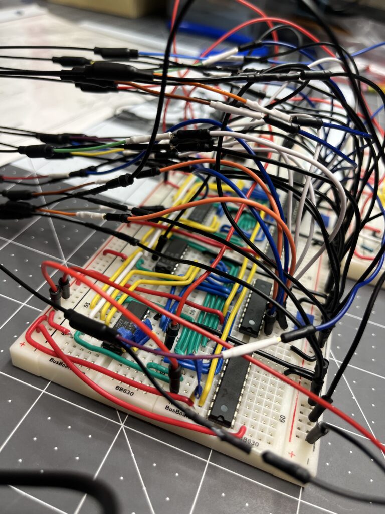
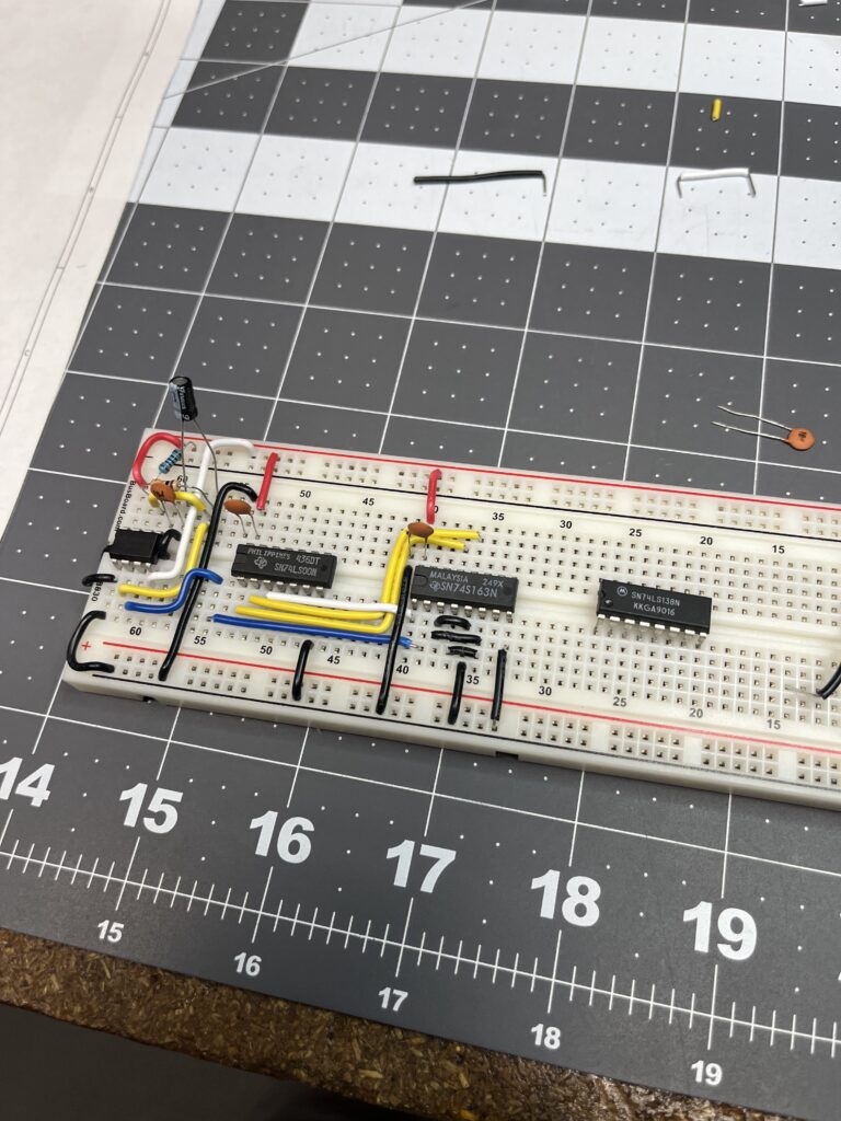
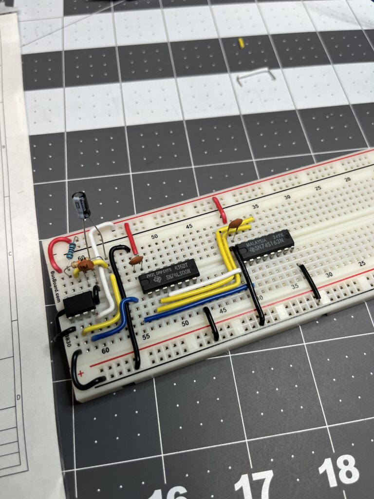
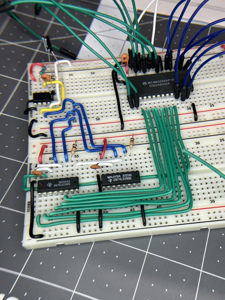
    The Memory Module integrates:

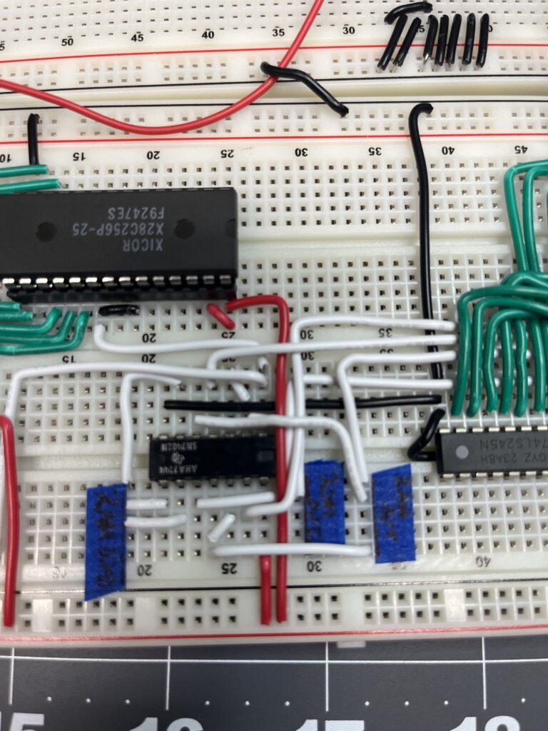
    • AT28C256 EEPROM: 32KB Program ROM containing instruction sequences
    • MCM60256 SRAM: 32KB RAM for data storage and manipulation
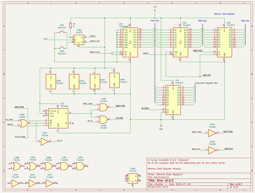
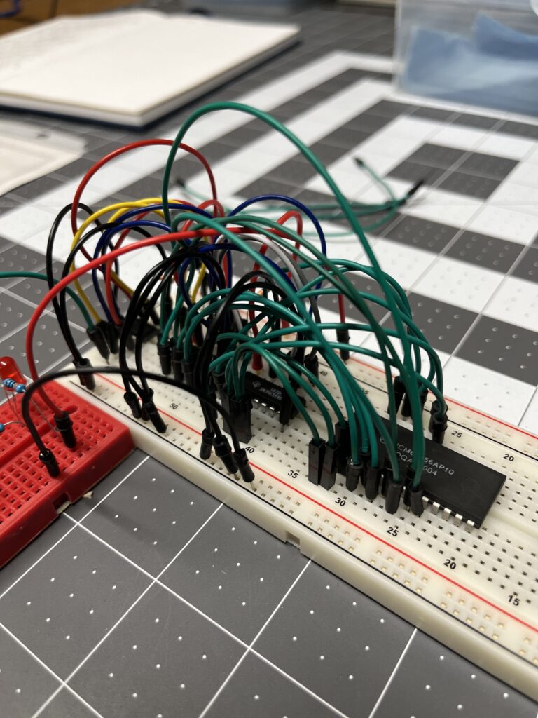
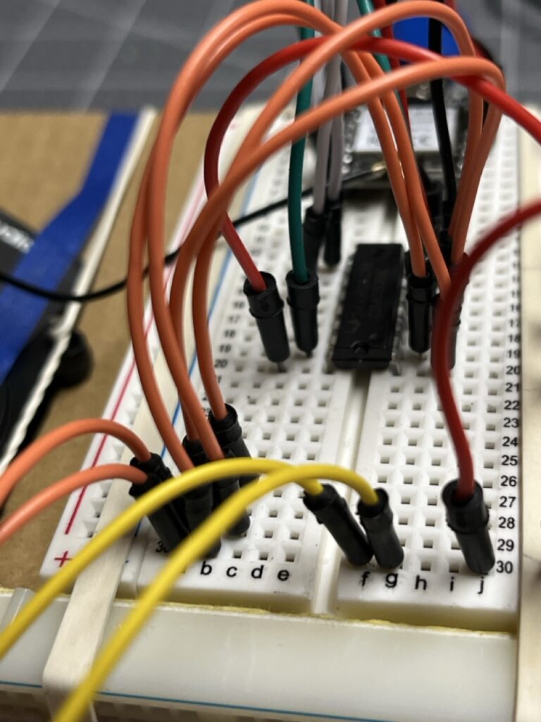
    • 74LS245 Bus Transceivers: Bidirectional buffers preventing bus contention
    • 74LS121 Monostable Multivibrator: Precision pulse generator for SRAM write timing
    • 16-bit Address Bus: Shared addressing for both ROM and RAM
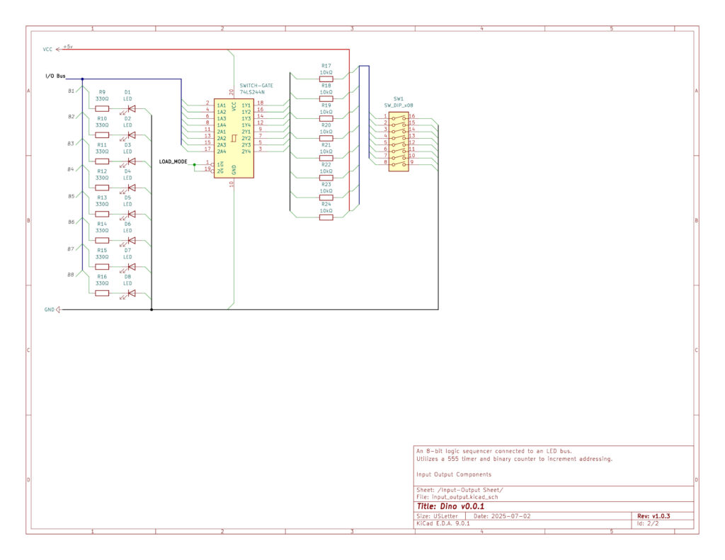
    • 8-bit Data Bus: Common data pathway with LED monitoring

    Bus Architecture and Arbitration

    The original design specified 74LS244 unidirectional buffers for ROM output. However, the 74LS245 bidirectional transceiver proved superior even for unidirectional operation, providing consistent pinout and better drive characteristics.

    Critical Discovery: I/O7 on both RAM and ROM chips represented the LSB, not the MSB as initially assumed. This revelation required rewiring the entire data bus interface to maintain consistent bit ordering across all modules. The discovery emerged during test rig construction when binary patterns didn’t match expected values.

    Bus Control Strategy:

    • ROM ‘245: DIR tied for output-only operation, OE controlled by ROM_OUT signal
    • RAM ‘245: DIR controlled by RAM_LOAD/RAM_OUT for bidirectional operation
    • Only one transceiver enabled at any time, preventing bus contention

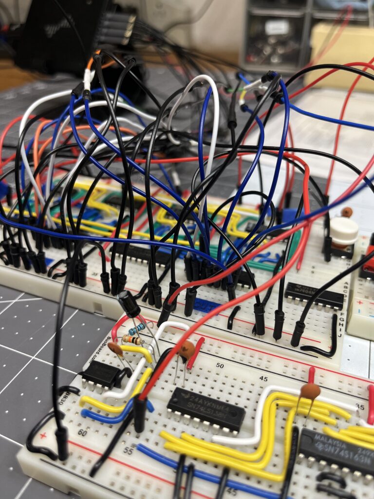
    The SRAM Write Timing Challenge

    Initial attempts to write SRAM using clock phase levels failed consistently. Investigation revealed that the MCM60256 SRAM requires an edge transition on its WE (Write Enable) pin to latch data, not a sustained level.

    Solution: Precision Pulse Generation

    The 74LS121 monostable multivibrator generates a 600ns active-low pulse:

    • Triggered simultaneously with other control signals
    • Provides setup time for data bus stabilization
    • Creates clean falling edge for SRAM write operation
    • Returns high before next clock phase

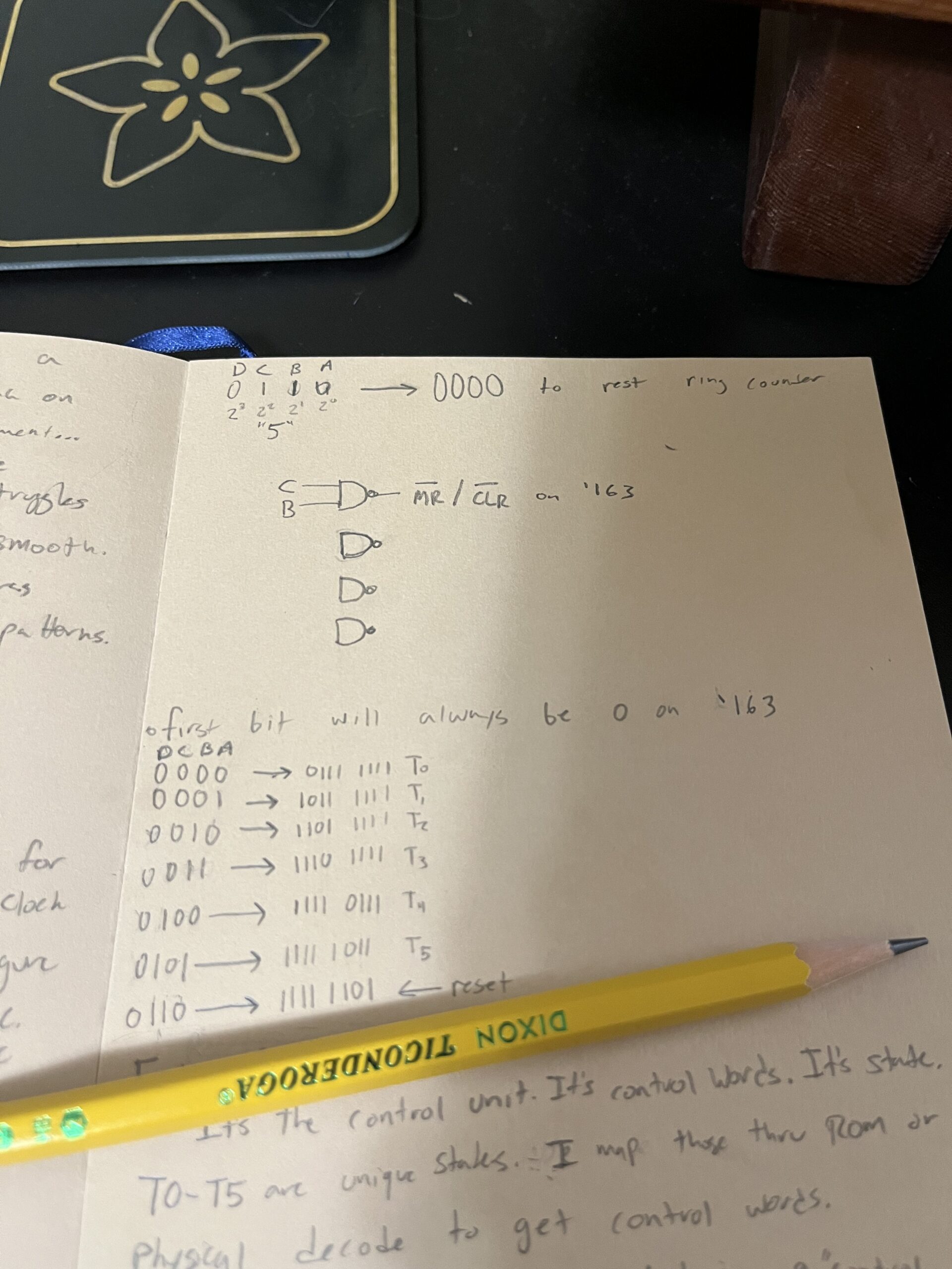
    RC Timing Calculation

    The 74LS121 pulse width calculation:

    t_pulse = 0.7 × R × C
    600ns = 0.7 × 10kΩ × C
    C = 86pF (100pF selected for margin)
    

    Implementation Note: Both A1 and B inputs required pull-up to VCC for reliable triggering. Initial attempts to use PULSE_REQ directly on the B input created indeterminate behavior.

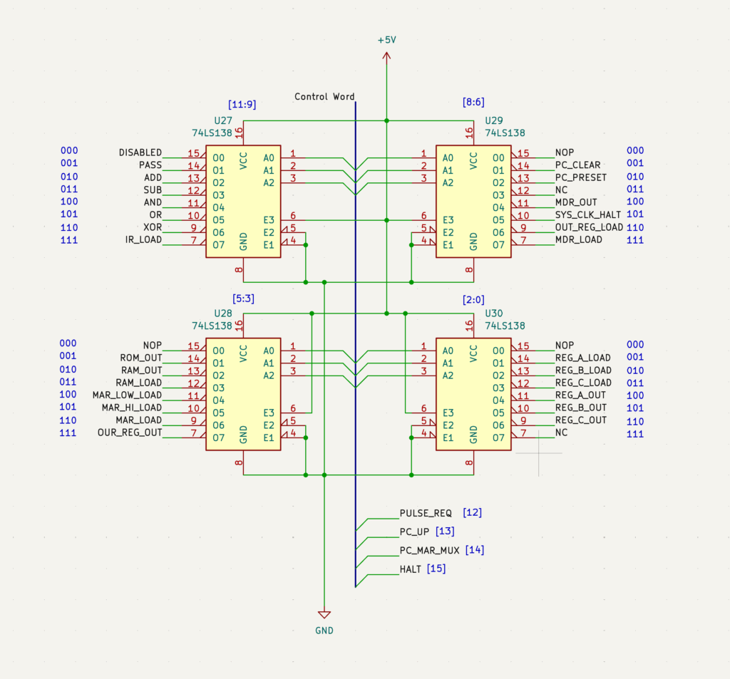
    Control Signal Architecture

    The Memory Module responds to four control bits from the Microcode Decoder:

    SignalFunctionSource
    ROM_OUTEnable ROM data onto busBank 2, Code 001
    RAM_OUTEnable RAM data onto busBank 2, Code 010
    RAM_LOADWrite bus data to RAMBank 2, Code 011
    PULSE_REQTrigger 121 for write pulseBit 12

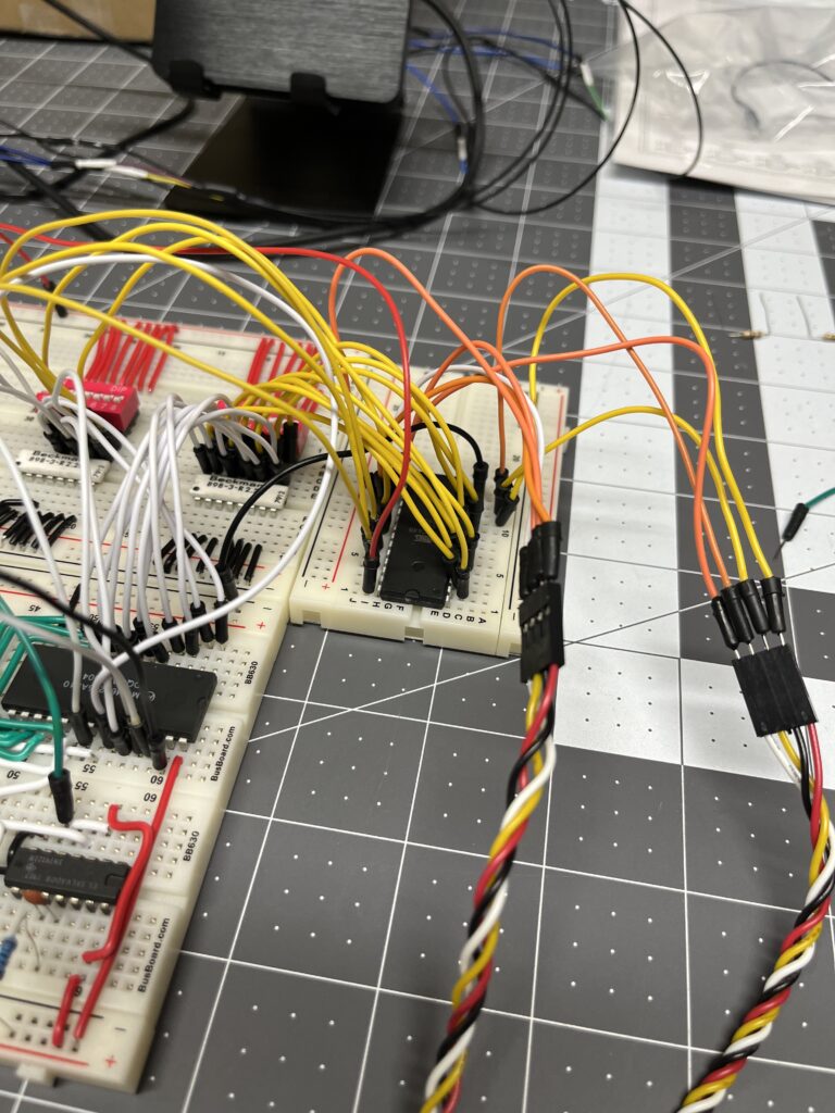
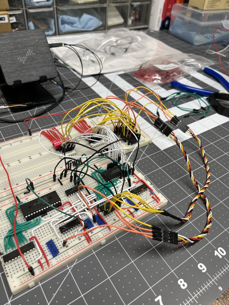
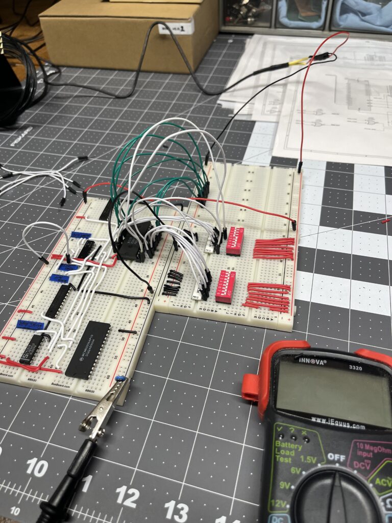
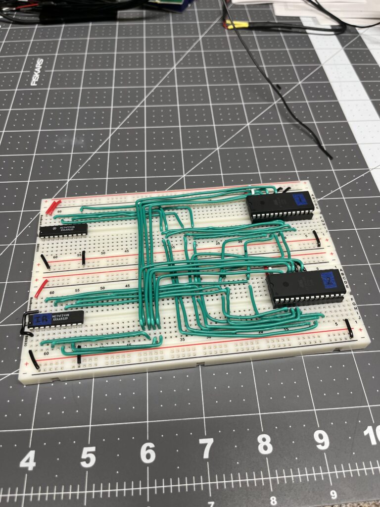
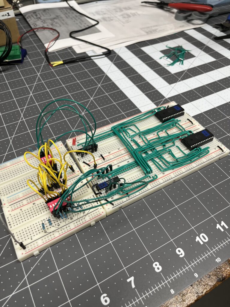
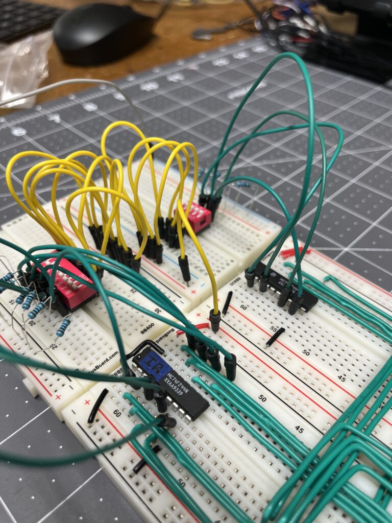
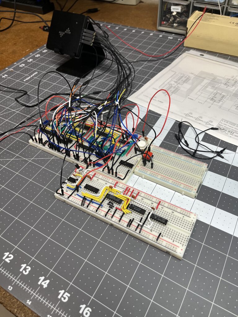
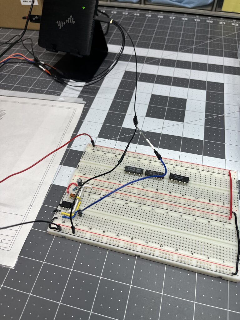
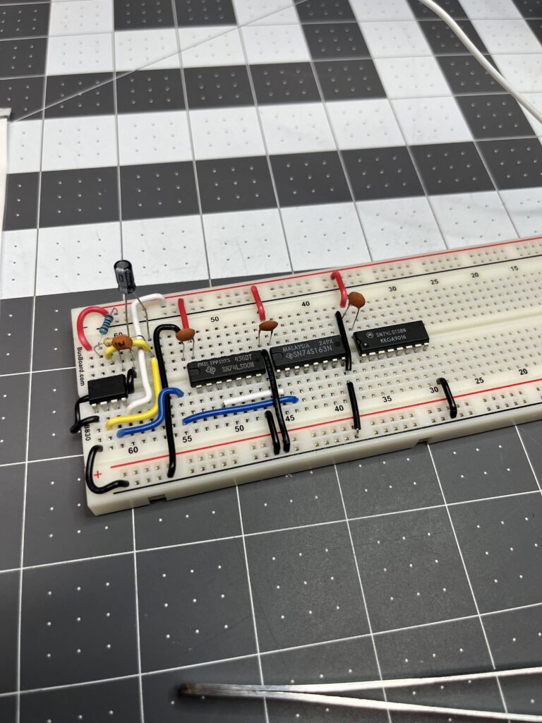
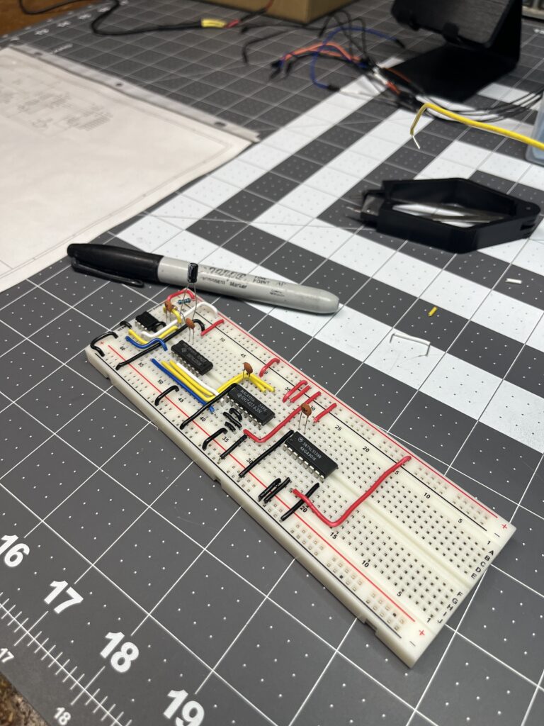
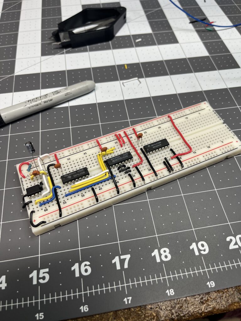
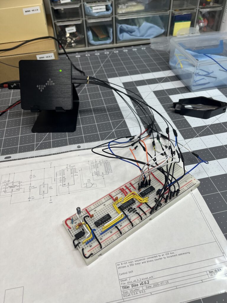
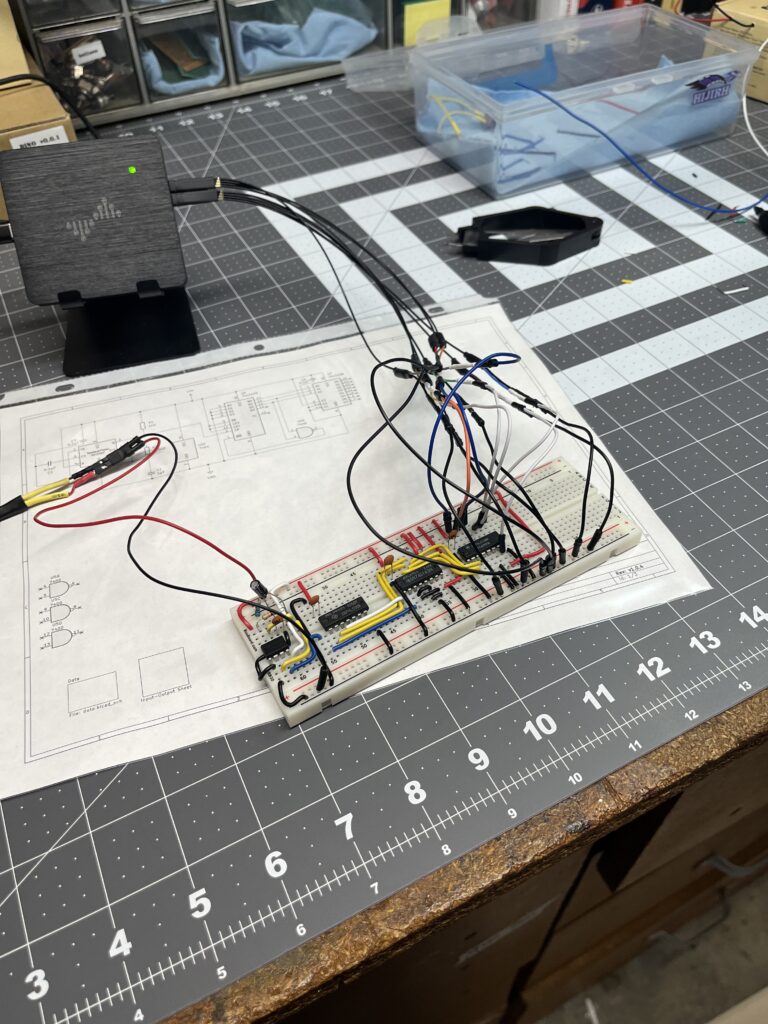
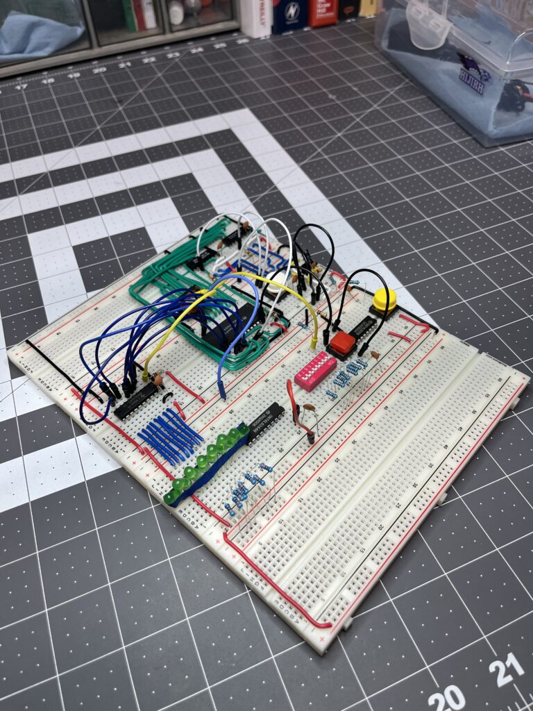
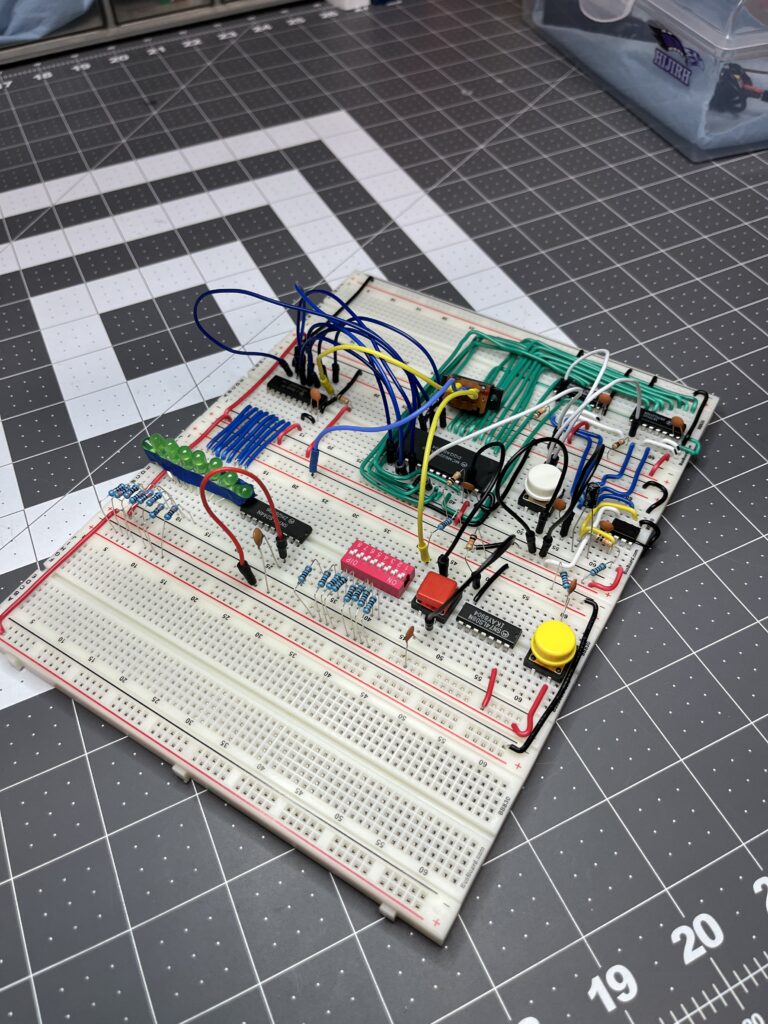
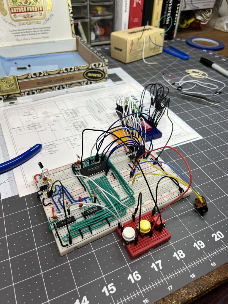
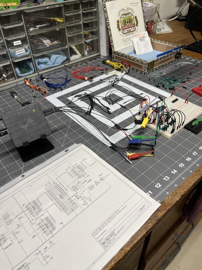
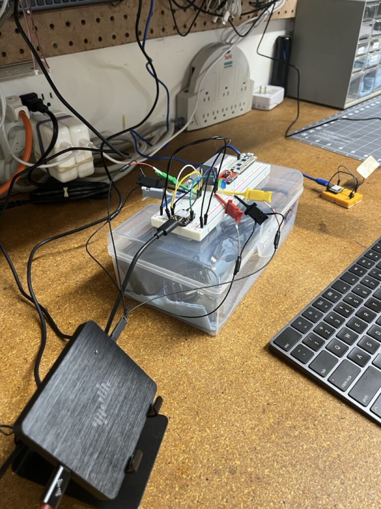
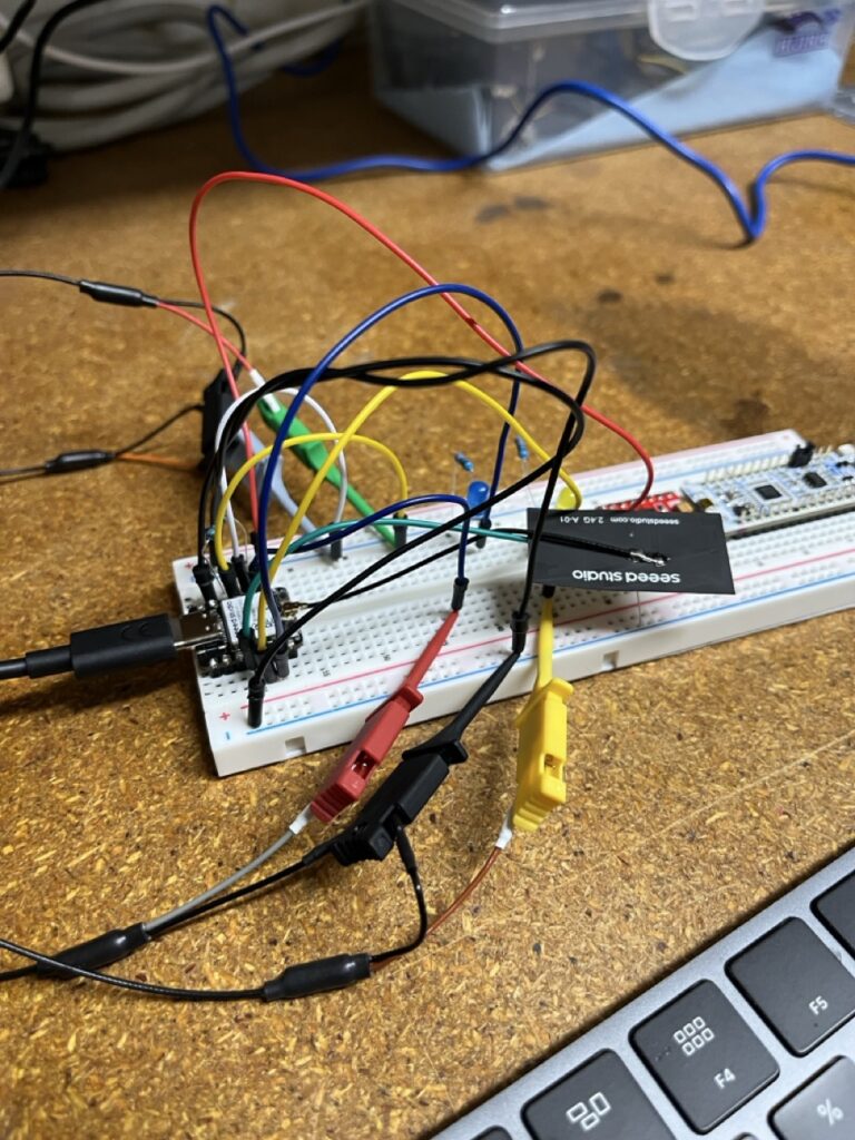
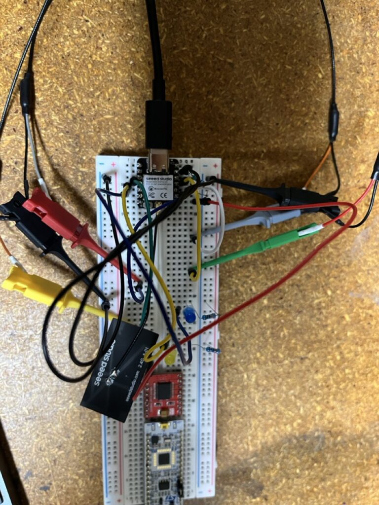
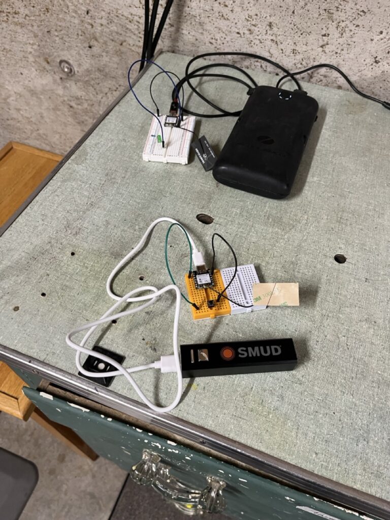
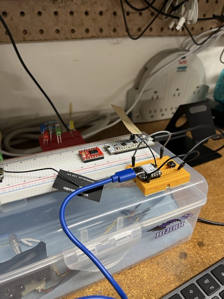
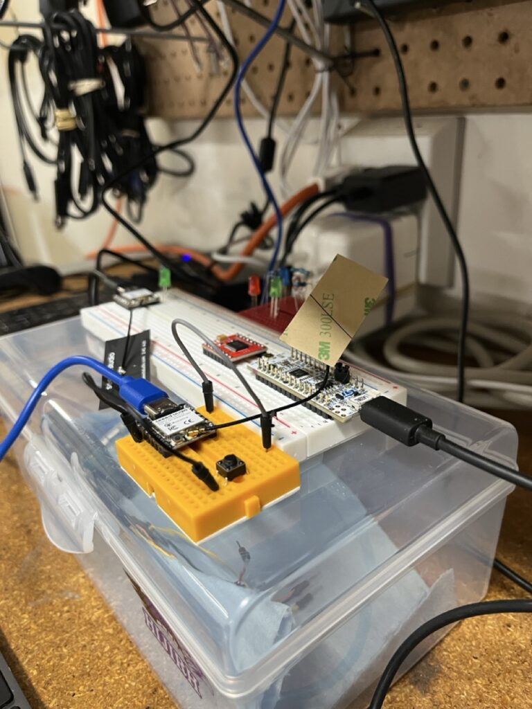
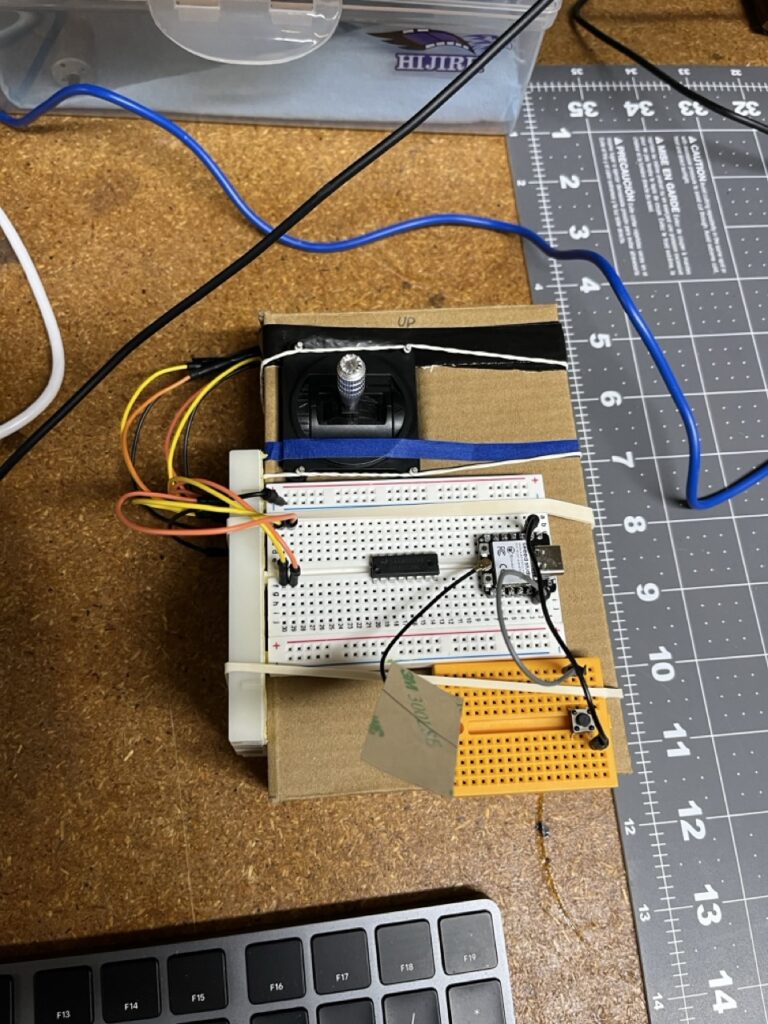
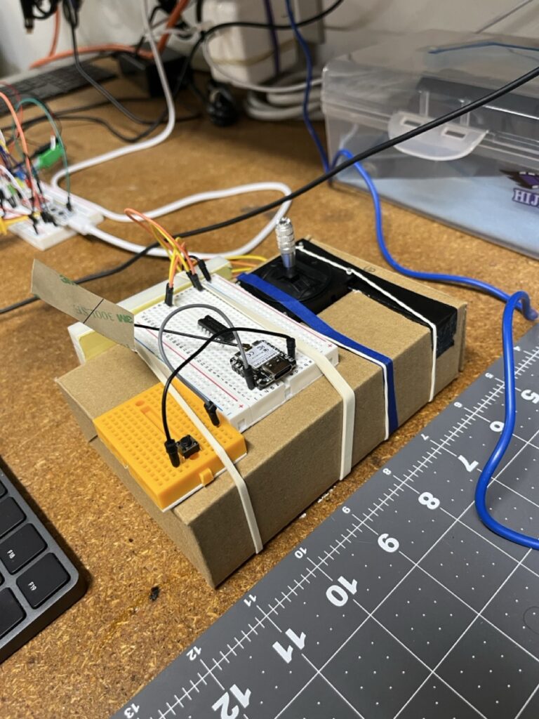
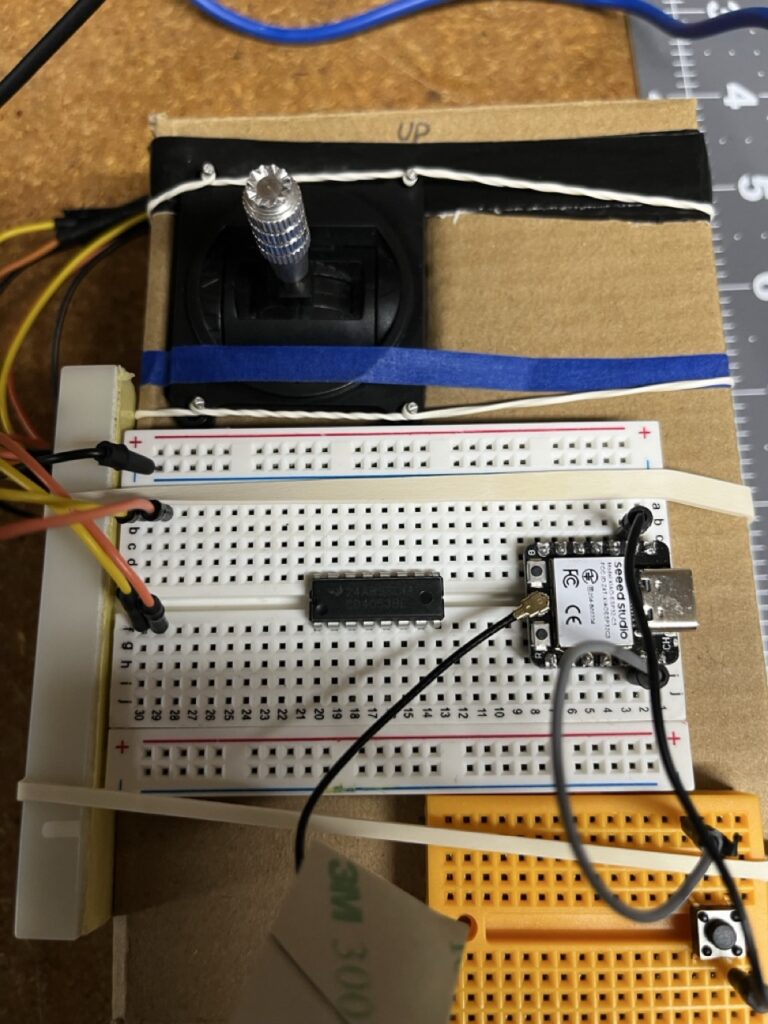
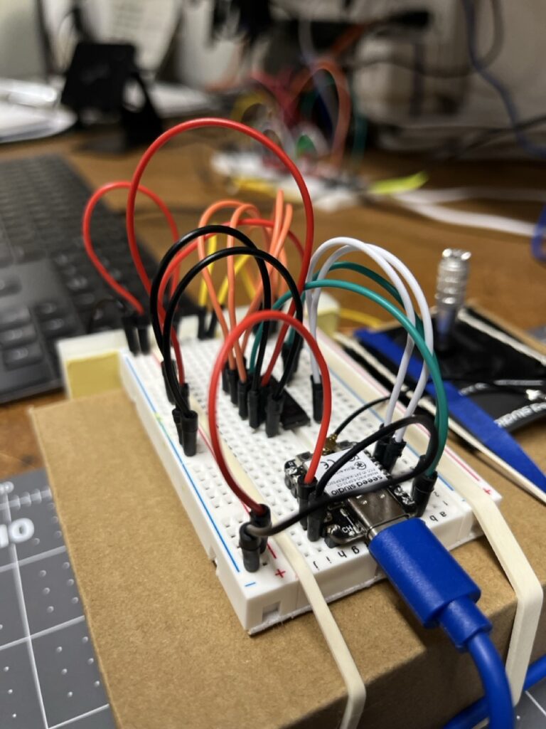
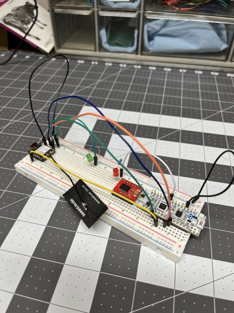
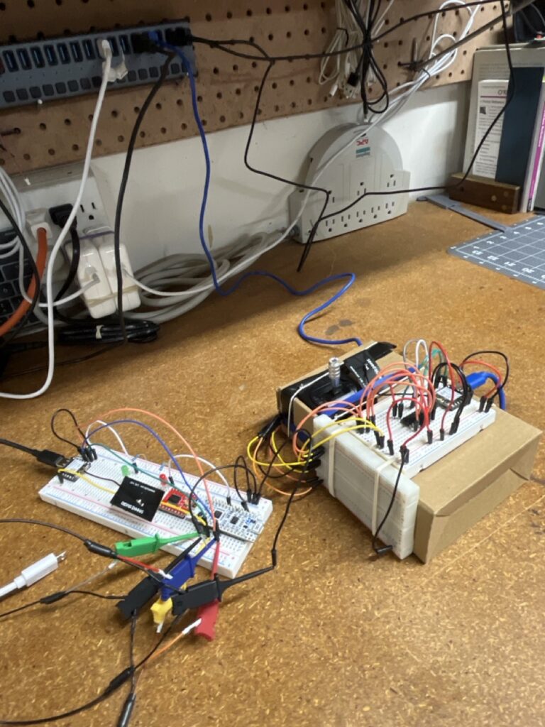
    Test Infrastructure Development

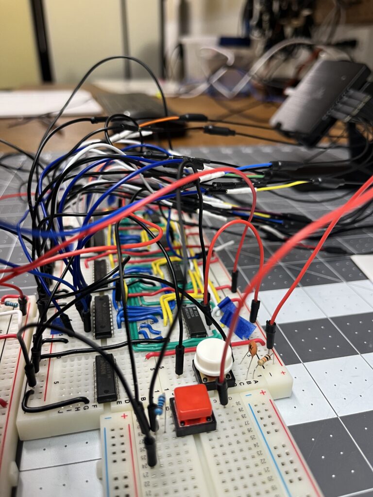
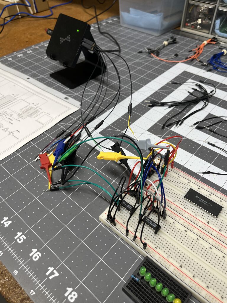
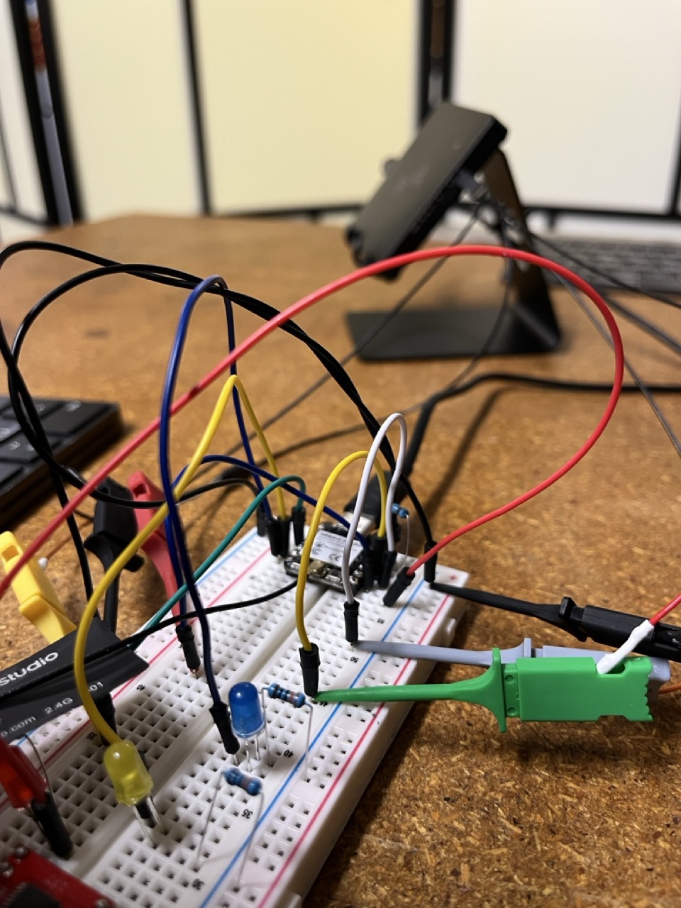
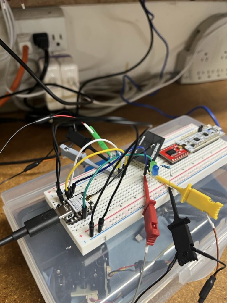
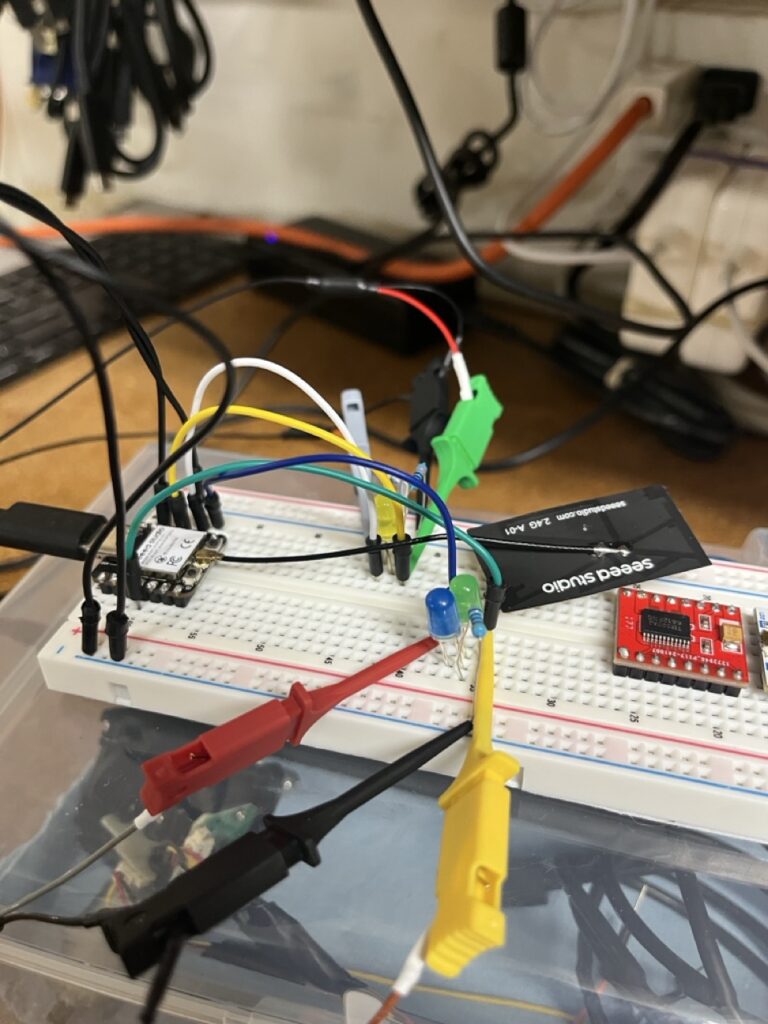
    Testing required sophisticated input and output monitoring:
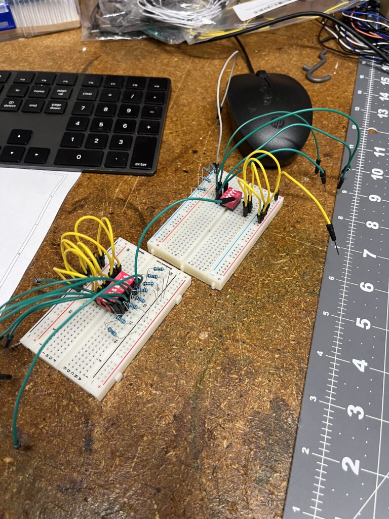
    Input Test Rig

    • 2 × 8-position DIP switches for manual address entry
    • Beckman 3.3kΩ resistor arrays for switch pull-down
    • Direct connection to 16-bit address bus

    Output Monitoring

    • 8 LEDs displaying current data bus state
    • 220Ω current-limiting resistors
    • Visual confirmation of read/write operations

    Test Methodology and Validation

    Dual Test Program Architecture

    Testing the Memory Module required two distinct C programs to validate both ROM and RAM operations independently:

    1. Program ROM Test: Verification of EEPROM read operations
    2. SRAM Test Controller: Coordinated write/read validation with proper control signal timing

    Program ROM Test Development

    The first C program generated test patterns for the AT28C256 EEPROM:

    // Key test addresses and values
    eeprom[0x0000] = 0xAA;  // Alternating bit pattern
    eeprom[0x0001] = 0x55;  // Inverse pattern
    eeprom[0x1234] = 0x12;  // Address-based value
    eeprom[0xABCD] = 0xCD;  // High address test
    

    Test ROM Mini-Microcode Controller

    The critical innovation was developing a dedicated Test ROM that acted as a miniature microcode controller specifically for SRAM testing. This second C program generated control word sequences that could:

    • Write data patterns to the bus
    • Assert RAM_LOAD simultaneously with PULSE_REQ
    • Coordinate RAM_OUT for read verification
    • Maintain proper control signal timing relationships

    This Test ROM approach better reflected actual system integration where the Microcode Decoder would generate all control signals simultaneously, rather than manual switch manipulation that could introduce timing skew.

    Systematic Test Sequence

    1. ROM_OUT Validation
      • Set DIP switches to test address
      • Assert ROM_OUT via Test ROM control pattern
      • Verify LED pattern matches burned EEPROM data
      • Confirmed: ROM data successfully appears on bus
    2. PULSE_REQ Verification
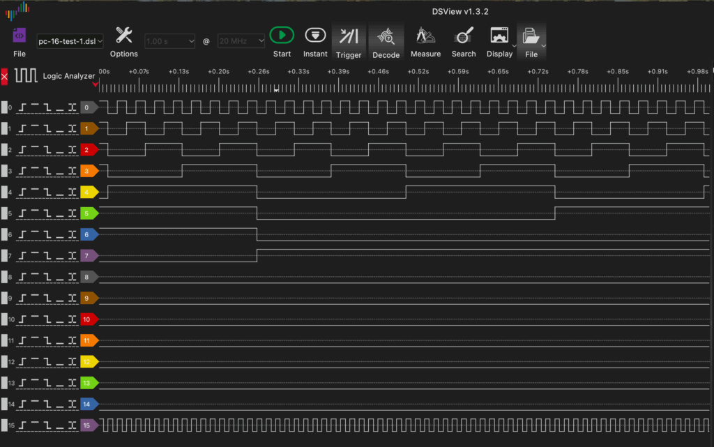
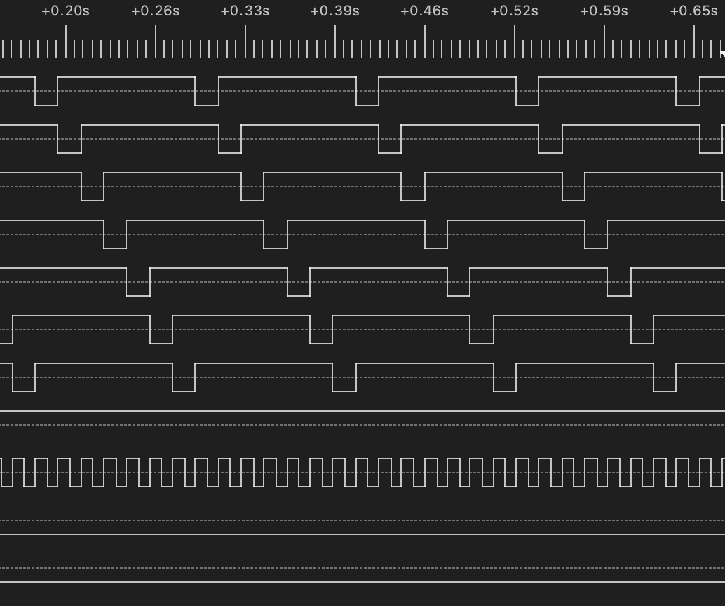
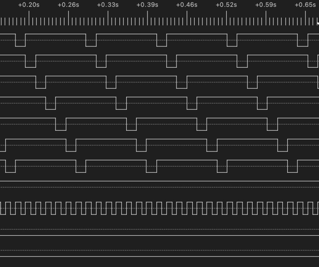
      • Test ROM generates PULSE_REQ signal
      • Monitor 74LS121 output with oscilloscope
      • Confirm 600ns pulse width with clean edges
      • Confirmed: Pulse generation operates within specifications
    3. RAM_LOAD Operation (via Test ROM)
      • Test ROM places data pattern on bus
      • Simultaneously asserts RAM_LOAD and PULSE_REQ
      • All control bits loaded in parallel, mimicking actual microcode operation
      • Confirmed: Data latched into SRAM as expected
    4. RAM_OUT Verification
      • Test ROM switches to read mode
      • Asserts RAM_OUT for previously written address
      • Compare bus output to written value
      • Confirmed: Complete write-read cycle functional

    The mini-microcode Test ROM validated that simultaneous control signal assertion worked correctly — a critical requirement for integration with the actual Microcode Decoder module.

    Debugging Discoveries

    Address Confusion Resolution

    Initial testing showed data corruption — writing to one address but reading incorrect values from another. Root cause: attempting to share the 16-bit address generator between test ROM reads and SRAM operations.

    Solution: Separate address generation for each test phase. This “classic case of trying to move too fast” reinforced the importance of methodical, isolated testing.

    Trigger Logic Refinement

    Original NOR gate configuration for 74LS121 triggering proved unreliable. Multiple schematic revisions led to a clean NAND gate implementation that provided deterministic pulse generation.

    Schematic Evolution

    The Memory Module underwent three major schematic revisions:

    1. Initial design with 74LS244 buffers and level-triggered writes
    2. Migration to 74LS245 transceivers with pulse generator addition
    3. Final refinement of trigger logic and pull-up configurations

    Each revision reflected lessons learned during hardware testing, demonstrating the iterative nature of discrete logic design.

    Engineering Insights

    The Memory Module implementation reinforced several critical principles:

    • Bit Ordering Discipline: Consistent LSB/MSB conventions across all modules prevents cascading debug sessions
    • Edge vs. Level Triggering: Understanding component timing requirements before design prevents fundamental architectural errors
    • Isolated Testing: Attempting to share test infrastructure between different operations creates confusion and masks real issues
    • RC Circuit Fundamentals: The 0.7 factor in 74LS121 timing calculations represents practical engineering constants that must be respected

    Milestone Confirmation

    The Memory Module is fully operational, providing:

    • Reliable ROM instruction fetches
    • Deterministic SRAM read/write cycles
    • Clean bus arbitration without contention
    • Validated timing margins for all operations

    Next Phase: Memory Data Register

    With the Memory Module complete, the next implementation is the Memory Data Register (MDR) — the critical buffer between memory operations and the CPU’s internal registers. The MDR will provide the temporary storage necessary for complex addressing modes and multi-cycle operations.

    The systematic progression continues: each module building upon validated foundations, methodically constructing a complete discrete logic computer from fundamental components.

  • DINO CPU Project – Microcode Decoder Module Implementation

    DINO CPU Project – Microcode Decoder Module Implementation

    The Control Word Generation Module

    Following the completion of the Program Counter module, the next critical milestone in the DINO CPU build was implementing the Microcode Decoder Module. This subsystem is the decoding bridge between the Program Counter, Instruction Register, and datapath — transforming a simple count and timing phases into precise sequences of control signals that orchestrate the CPU’s fetch–decode–execute cycle.

    This marks a shift in the project’s pace: we are now working with deliberate, methodical engineering discipline. No longer in discovery mode, each module is designed on paper, validated logically, then wired and tested against clearly defined criteria before being declared operational.


    Architectural Role

    The Microcode Decoder accepts:

    • Timer Phase from the ring counter
    • Instruction Opcode from the Instruction Register

    These form a 16-bit address into a parallel EEPROM pair:

    • ROM #1: upper byte
    • ROM #2: lower byte

    Example: address 0xBEEF would store 0xBE in ROM #1 and 0xEF in ROM #2. The output directly drives the control lines of the CPU via decoder banks, enabling deterministic hardware sequencing.


    Hardware Selection

    • ROMs: 2 × AT28C64 8-KB EEPROMs, wired in parallel for 16-bit output
    • Decoders: 4 × 74LS138N 3-to-8 demultiplexers to split the 16 control word bits into functional banks, with 4 additional lines reserved for signals that are not mutually exclusive with other control bits.
    • Pulse Generation: 74LS121 monostable multivibrators for intra-phase latching

    ISA Revision and Bit-Ordering Correction

    Early in design, the instruction set was built with the first bit as MSB, but the hardware required it as LSB. Correcting this forced schematic revisions, but clarified the logical flow from opcode to control word.

    Current Instruction Set:

    LDAI, LDBI, STA, STB, NOP, LDA, ADD, MOV, OUT, HLT

    These instructions form the minimum set needed to verify memory transfers, register operations, arithmetic, and output control.


    Control Word Matrix

    The Microcode Decoder produces a 16-bit control word, organized into functional groups:

    Bit(s)Function / Decoder BankCodes & Meanings
    15HALTStart the next phase early
    14MAR_PC_MUXUse MAR or PC as address source for IR
    13PC_UPIncrement Program Counter
    12PULSE_REQ (new)Intra-phase pulse trigger
    11:9Bank 4: ALU Ops000: ALU Disabled
    001: Pass Accumulator
    010: ADD
    011: SUB
    100: AND
    101: OR
    110: XOR
    111: IR_LOAD
    8:6Bank 3: Program Counter Control000: NOP
    001: PC_CLEAR
    010: PC_PRESET
    011: unused
    100: MDR_OUT
    101: SYS_HALT
    110: OUT_REG_LOAD
    111: unused
    5:3Bank 2: Memory Ops000: NOP
    001: ROM_OUT
    010: RAM_OUT
    011: RAM_LOAD
    100: MAR_LO_LOAD
    101: MAR_HI_LOAD
    110: MAR_LOAD
    111: OUT_REG_OUT
    2:0Bank 1: Register Ops000: NOP
    001: REG_A_LOAD
    010: REG_B_LOAD
    011: REG_C_LOAD
    100: REG_A_OUT
    101: REG_B_OUT
    110: REG_C_OUT
    111: MDR_LOAD

    The PULSE_REQ Discovery

    While defining the control word matrix, it became clear that certain latch operations could not reliably complete within a full T-phase. Halting and latching data simultaneously left uncertainty about whether the latch would capture stable data.

    Solution: Introduce an intra-phase pulse (PULSE_REQ) generated by a 74LS121 to trigger latches early enough for guaranteed stability — essential for RAM writes and 74LS373 register loads.


    Boot Sequence Strategy

    • Microcode Addresses 0x0000–0x000F: Reserved for boot sequence
    • Reset mode forces opcode 0x00 into the IR via a 74LS244 buffering hardwired zeros
    • JK flip-flop (74LS73) keeps the opcode at 0x00 until reset mode is released
    • At 0x0000: Microcode resets the PC
    • At 0x000F: PC is incremented
    • IR loads new opcodes only after reset mode ends

    Schematic Development

    The Microcode Decoder and the next modules (MDR, IR, Memory, Registers) have been fully drafted in KiCAD to ensure logical consistency before wiring.


    Test Strategy

    Testing verified correct EEPROM byte pairing for given addresses. DIP switches simulated opcode + timer phase. A multimeter was used to measure each ROM output pin, as the static conditions made it easier than a logic analyzer. Measurements were recorded in the engineering journal and compared to expected binary/hex values.

    Test steps:

    1. Set DIP switches for desired address
    2. Measure each ROM output with multimeter
    3. Record voltage levels, convert to binary/hex
    4. Compare with EEPROM binary file contents
    5. Repeat for all patterns
    AddressROM #1 (High Byte)ROM #2 (Low Byte)
    0x00000xDE0xAD
    0x00010xBE0xEF
    0x0DED0xBE0xEF
    0x0FED0xFE0xED

    Two C programs supported test and verification:

    test.c

    
    /**
     * test.c - Parallel EEPROM test data generator for DINO
     *
     * This program generates two binary files (eeprom1.bin and eeprom2.bin)
     * for burning into two parallel EEPROMs used in the DINO hardware project.
     *
     * Each file is 4096 bytes (0x1000) and specific values are written at key addresses:
     *   - eeprom1.bin: 0xDE at 0x0000, 0xBE at 0x0001, 0xBE at 0x0DED, 0xFE at 0x0FED
     *   - eeprom2.bin: 0xAD at 0x0000, 0xEF at 0x0001, 0xEF at 0x0DED, 0xED at 0x0FED
     *
    #
    # Usage:
    #   To compile:
    #     gcc test.c -o test
    #
    #   To generate the EEPROM files:
    #     ./test
    #
    #   To check the contents of each bin file:
    #     hexdump -C eeprom1.bin
    #     hexdump -C eeprom2.bin
    #
    #   How to read the output:
    #     - The address at the start of each line (e.g., 00000fe0) is the starting offset for that line.
    #     - Each line shows 16 bytes, so the first byte is at the line's address, the second at address+1, etc.
    #     - To find a specific address (e.g., 0x0FED), calculate its position: 0x0FE0 + 13 = 0x0FED (13th byte in the line).
    #     - Count bytes from left to right, starting at 0 for each line.
    #     - Example: If you see 'fe' as the 13th byte on the line starting with 00000fe0, that's the value at 0x0FED.
    #
     * All other bytes are zero-filled. This is for hardware and microcode testing.
     */
    #include <stdio.h>
    #include <stdint.h>
    
    int main(void) {
        FILE *f1 = fopen("eeprom1.bin", "wb");
        FILE *f2 = fopen("eeprom2.bin", "wb");
        if (!f1 || !f2) {
            perror("Failed to open one of the files");
            if (f1) fclose(f1);
            if (f2) fclose(f2);
            return 1;
        }
        uint8_t eeprom1[0x2000] = {0};
        uint8_t eeprom2[0x2000] = {0};
    
        // Fill both EEPROMs with zeros
        for (int i = 0; i < sizeof(eeprom1); i++) {
            eeprom1[i] = 0x00;
            eeprom2[i] = 0x00;
        }
    
        // Write 0xDE at 0x0000 in eeprom1
        eeprom1[0x0000] = 0xDE;
        // Write 0xAD at 0x0000 in eeprom2
        eeprom2[0x0000] = 0xAD;
    
        // Write 0xBE at 0x0001 in eeprom1
        eeprom1[0x0001] = 0xBE;
        // Write 0xEF at 0x0001 in eeprom2
        eeprom2[0x0001] = 0xEF;
    
        // Write 0xBA at 0x0002 in eeprom1
        eeprom1[0x0002] = 0xBA;
        // Write 0xBE at 0x0002 in eeprom2
        eeprom2[0x0002] = 0xBE;
    
        // Write 0xBE at 0x0DED in eeprom1
        eeprom1[0x0DED] = 0xBE;
    
        // Write 0xEF at 0x0DED in eeprom2
        eeprom2[0x0DED] = 0xEF;
    
        // Write 0xCA at 0x0003 in eeprom1
        eeprom1[0x0003] = 0xCA;
        // Write 0xFE at 0x0003 in eeprom2
        eeprom2[0x0003] = 0xFE;
    
        // Write 0xFE at 0x0FED in eeprom1
        eeprom1[0x0FED] = 0xFE;
        // Write 0xED at 0x0FED in eeprom2
        eeprom2[0x0FED] = 0xED;
    
        fwrite(eeprom1, sizeof(uint8_t), sizeof(eeprom1), f1);
        fwrite(eeprom2, sizeof(uint8_t), sizeof(eeprom2), f2);
        fclose(f1);
        fclose(f2);
        return 0;
    }

    verify.c

    /**
     * verify.c - Verifies specific addresses in eeprom1.bin and eeprom2.bin
     *
     * This program reads eeprom1.bin and eeprom2.bin, then prints the values at key addresses:
     *   - 0x0000, 0x0001, 0x0002, 0x0003, 0x0DED, 0x0FED
     *
     * Output format:
     *   EEPROM1[0xADDR] = 0xXX
     *   EEPROM2[0xADDR] = 0xXX
     *
     * Usage:
     *   gcc verify.c -o verify
     *   ./verify
     */
    #include <stdio.h>
    #include <stdint.h>
    #include <stdlib.h>
    
    #define EEPROM_SIZE 0x2000
    
    int main(void) {
        const char *fname1 = "eeprom1.bin";
        const char *fname2 = "eeprom2.bin";
        FILE *f1 = fopen(fname1, "rb");
        FILE *f2 = fopen(fname2, "rb");
        if (!f1 || !f2) {
            perror("Failed to open one of the EEPROM files");
            if (f1) fclose(f1);
            if (f2) fclose(f2);
            return 1;
        }
        uint8_t eeprom1[EEPROM_SIZE];
        uint8_t eeprom2[EEPROM_SIZE];
        if (fread(eeprom1, 1, EEPROM_SIZE, f1) != EEPROM_SIZE) {
            fprintf(stderr, "Error reading %s\n", fname1);
            fclose(f1); fclose(f2);
            return 2;
        }
        if (fread(eeprom2, 1, EEPROM_SIZE, f2) != EEPROM_SIZE) {
            fprintf(stderr, "Error reading %s\n", fname2);
            fclose(f1); fclose(f2);
            return 3;
        }
        fclose(f1);
        fclose(f2);
    
        uint16_t addresses[] = {0x0000, 0x0001, 0x0002, 0x0003, 0x0DED, 0x0FED};
        size_t n = sizeof(addresses)/sizeof(addresses[0]);
        printf("EEPROM Verification Results:\n");
        for (size_t i = 0; i < n; ++i) {
            printf("EEPROM1[0x%04X] = 0x%02X\n", addresses[i], eeprom1[addresses[i]]);
            printf("EEPROM2[0x%04X] = 0x%02X\n", addresses[i], eeprom2[addresses[i]]);
        }
        return 0;
    }

    Burn & Verification

    • EEPROMs written with a GECU T48 programmer via minipro
    • ROM #1 programmed with high byte file, ROM #2 with low byte file
    • Multiple rewire/re-burn cycles until outputs matched expected values

    Milestone Achievement

    The Microcode Decoder is fully functional. It bridges the Program Counter and upcoming MDR/IR stages, converting opcodes and timing into precise control signals for the CPU.


    Engineering Methodology

    This build reinforced:

    • Correcting data representation early prevents cascading errors
    • PULSE_REQ improved timing integrity and latch reliability
    • Static signal verification with a multimeter can be more effective than a logic analyzer for certain tests
    • Pre-drafting future modules ensures coherent datapath planning

    Next Steps

    1. Memory Data Register (MDR) – temporary storage for memory read/writes
    2. Instruction Register (IR) – holds current opcode for decoding
    3. Memory Module & Register Module – completes the execution datapath
  • DINO CPU Project – Program Counter Implementation and Validation

    DINO CPU Project – Program Counter Implementation and Validation

    The Critical Address Generation Foundation

    With the ring counter establishing systematic timing coordination, the DINO CPU project reached a pivotal engineering milestone: implementing the 16-bit Program Counter that would serve as the addressing backbone for all instruction execution. This module demanded cascaded counter logic with bidirectional operation, preset capability, and clean bus arbitration – functionality that would make or break the entire discrete logic computer.

    The engineering challenge centered on coordinating four 74LS193 counters through 74LS245 bus transceivers while maintaining signal integrity across a complex 16-bit address architecture.


    Schematic Architecture and Component Analysis

    Strategic Component Selection

    The PC implementation required components that could handle complex addressing requirements:

    • 74LS193 Quad Counters: Chosen for bidirectional counting with independent up/down clocks and comprehensive preset functionality
    • 74LS245 Bus Transceivers: Essential for bidirectional bus control and output enable coordination
    • 74LS02 NOR Gate: Provides active-low signal inversion required for control word compatibility

    Circuit Complexity Evolution

    The schematic development represented the most intricate circuit design attempted to date. Initial architecture included a 74LS32 OR gate for PC_MUX decode logic, but systematic analysis revealed this was redundant – the control word matrix already provided the necessary logic states.

    This optimization eliminated unnecessary components while simplifying the signal routing:

    • Iteration 1: Complete counter cascade with redundant decode logic
    • Iteration 2: Streamlined design with OR gate removal and corrected DIR signals on output transceivers

    The final schematic achieved maximum functionality with minimal component count through careful architectural analysis.


    Systematic Testing Protocol Development

    Comprehensive Validation Framework

    Rather than hoping the complex circuit would work, a rigorous testing protocol was established before construction began:

    • Preset Operations: Verify PC responds correctly to PC_PRESET control activation
    • Increment Coordination: Validate carry propagation across all four 74LS193 stages
    • Decrement Functionality: Confirm borrow propagation through systematic countdown testing
    • Bus Arbitration: Ensure PC_MUX properly controls output transceiver states
    • Isolated Operation: Verify counter maintains function when bus outputs are disabled
    • Full-Range Capability: Test 16-bit counting across complete address space

    This methodology ensured any failures could be traced to specific subsystems rather than requiring wholesale circuit debugging.


    Construction Strategy and Pattern Recognition

    Wiring Complexity Management

    The 16-bit bus architecture demanded strategic construction planning beyond typical breadboard assembly:

    • Dupont Jumper Pre-Fitting: Temporary connections identified potential wire routing conflicts before permanent installation
    • Component Placement Optimization: Alternating input and output transceivers created natural wiring symmetries
    • Pattern-Based Routing: Systematic cascade connections reduced complexity through visual consistency

    Engineering Discovery

    The construction process revealed how thoughtful component arrangement transforms chaotic wiring into organized patterns. Alternating transceiver placement created identical routing for all cascade connections, turning potential complexity into systematic regularity.

    The result resembled engineered artwork – clean, predictable wire patterns that facilitated both construction and debugging.


    Validation Results and System Integration

    Logic Analyzer Verification

    Complete 16-bit bus monitoring provided comprehensive visibility into counter operations:

    • Immediate Success: All functionality operational on first power-up attempt
    • Clean Transitions: No timing glitches or signal integrity issues observed
    • Proper Cascading: Carry and borrow signals propagating correctly across all stages

    Timing Dependency Resolution

    Testing revealed critical insights about cascade signal timing requirements:

    • Manual Control Limitations: Hand-operated up/down controls provided insufficient pulse width for cascade operations
    • 555 Timer Integration: 60Hz clock delivered proper timing characteristics for ~BO/~CO signals
    • Engineering Insight: Cascade functionality depends on clock pulse duration, not merely edge timing

    Preset Capability Confirmation

    Address loading validation completed the testing sequence:

    • MSB Testing Strategy: Preset testing focused on high-order bits for immediate visual confirmation
    • Construction Error Discovery: Input transceivers inadvertently hardwired during assembly process
    • Rapid Resolution: Single connection correction restored full preset functionality

    Engineering Significance and System Foundation

    Complexity Management Success

    The PC implementation validated key embedded development principles:

    • Schematic-Driven Development: KiCAD circuit design prevented construction errors and enabled strategic component placement
    • Systematic Validation: Pre-construction testing framework eliminated debugging uncertainty
    • Methodical Assembly: Disciplined wiring approach prevented the chaos typical of complex breadboard circuits

    Architectural Foundation Establishment

    Successful PC operation provides the addressing infrastructure for complete CPU functionality:

    • Instruction Sequencing: Reliable program advancement enables systematic instruction execution cycles
    • Address Space Access: 16-bit capability provides substantial memory addressing range
    • Control Word Integration: PC_MUX and PC_PRESET signals interface cleanly with established timing architecture

    Methodology Validation

    This milestone demonstrated how systematic engineering practices produce reliable results on complex multi-chip coordination problems. The combination of thorough design analysis, strategic testing protocols, and disciplined construction yielded first-attempt success on challenging timing-dependent hardware.


    Development Trajectory: T0/T1 Decoder Implementation

    The proven Program Counter establishes reliable address generation for the next critical phase:

    • Universal Instruction Fetch: T0/T1 timing states will coordinate ROM-to-IR data movement
    • Address Matrix Formation: Instruction Register output combined with ring counter states for control word indexing
    • Bootstrap Sequence Architecture: Initial fetch capability enabling instruction execution without manual startup

    The PC success provides engineering confidence for tackling the address formation complexity ahead.

    Core Engineering Principle: Complex embedded systems achieve reliability through systematic subsystem validation before integration attempts. The Program Counter milestone exemplifies how disciplined analysis, careful construction, and comprehensive testing enable first-try success on demanding multi-chip timing coordination challenges.

    The discrete logic computer advances toward complete computational capability through proven engineering methodology.

  • DINO CPU Project – Ring Counter Implementation and Control Unit Architecture

    DINO CPU Project – Ring Counter Implementation and Control Unit Architecture

    From Theory to Working Hardware

    With the control unit revelation providing clear direction for systematic timing coordination, the next phase involved translating architectural understanding into working hardware. The ring counter represents the timing heart that enables control word coordination – transforming the theoretical framework into practical implementation.

    The goal was to build the systematic T0-T5 timing sequence that would drive control word lookups and instruction execution phases.

    Ring Counter Implementation

    Hardware Components

    • 74LS163: 4-bit synchronous counter (binary sequence generation)
    • 74LS138: 3-to-8 decoder (converts binary count to one-hot timing signals)
    • 74LS00: NAND gate (detects count=6 to trigger reset)
    • NE555P: Timer circuit (proven from previous sequencer design)

    Circuit Operation

    The implementation creates a systematic T0→T1→T2→T3→T4→T5→reset timing sequence:

    Reset Logic: When the counter reaches binary 110 (decimal 6), both QB and QC outputs go HIGH. The NAND gate detects this condition and outputs LOW, triggering the ‘163’s active-low CLR input. The counter immediately resets to 000, creating the ring behavior.

    Decoder Output Pattern: The ‘138 decoder creates the required one-hot sequence with active-low outputs:

    • 000 (T0): Y0=LOW → 0111 1111
    • 001 (T1): Y1=LOW → 1011 1111
    • 010 (T2): Y2=LOW → 1101 1111
    • 011 (T3): Y3=LOW → 1110 1111
    • 100 (T4): Y4=LOW → 1111 0111
    • 101 (T5): Y5=LOW → 1111 1011

    Logic Analyzer Validation

    The ring counter was validated using logic analyzer capture, confirming:

    • Six distinct timing states: Clean T0→T1→T2→T3→T4→T5 sequence
    • Reset behavior: 7th state triggers reset pulse, immediately returns to T0
    • Timing consistency: Each state lasts approximately 60ms (consistent with 555 timing)
    • Signal integrity: Clean edges, proper logic levels, no glitches
    • Stable operation: Continuous cycling without timing irregularities

    The systematic T0-T5 timing states provide the foundation needed for control word generation and instruction sequencing.

    Architecture Planning and Component Selection

    Control Unit Evolution

    The successful ring counter implementation enabled architectural planning for the complete control unit system:

    Memory Architecture Defined:

    • 0x0000-0x0FFF: Control word table (4KB)
    • 0x1000-0xFFFF: Program space (60KB)
    • Parallel AT28C256 ROMs: 16-bit control words and instructions

    Instruction Register Implementation:

    • Two 74LS373: 8-bit transparent latches configured for 16-bit instruction storage
    • T1 control: LE signal derived from inverted T1 timing state
    • Stable operation: Transparent during T1 (instruction fetch), latched during T2-T6 (execute)

    Expandability Considerations

    The current 6-state ring counter can be expanded to 7 states by changing the reset detection logic:

    • Current: Detect count=6 (QB AND QC)
    • Future: Detect count=7 (QB AND QC AND QD) using 74LS10 triple 3-input NAND

    Engineering Methodology Validation

    This implementation phase validated several critical embedded development practices:

    • Component isolation testing: Ring counter validated independently before system integration
    • Logic analyzer verification: Hardware-level visibility essential for timing validation
    • Systematic problem resolution: Theoretical analysis confirmed by practical measurement
    • Proven building blocks: Timer circuit preserved from working sequencer design

    Next Phase Preparation

    The ring counter milestone establishes the timing foundation for control word matrix implementation. With systematic T0-T5 timing generation validated, the next development phase involves:

    • Control word architecture: ROM-based lookup table implementation
    • Instruction register integration: 16-bit instruction storage and decode
    • Data path coordination: Register, ALU, and memory interface control

    The control unit timing heart is operational. The systematic approach from proven ring counter timing → control word architecture → complete CPU represents solid engineering methodology where each phase builds on validated previous work.

    Memory Architecture Discovery

    The ring counter implementation sparked investigation into memory organization and system architecture. Several key insights emerged:

    Data Flow Architecture: The systematic data movement follows ROM→RAM→Register pathways rather than direct ROM→Register connections. This staging approach enables proper timing coordination where ROM data is first loaded into RAM workspace, then selectively moved to registers during appropriate timing states. SRAM provides the essential intermediate storage that allows the control unit to coordinate complex multi-step data transfers, while registers (74LS373) provide the parallel access needed for immediate decoder input and ALU operations.

    Parallel ROM Configuration: Two AT28C256 ROMs configured in parallel create 32K × 16-bit memory space rather than 64KB total capacity. This configuration provides 16-bit instruction words and control words while maintaining single-address access. The parallel approach eliminates the complexity of interleaved addressing while maximizing control word capability.

    Memory Map Strategy: Partitioning the 32K address space into control word table (0x0000-0x0FFF) and program storage (0x1000-0xFFFF) enables systematic ROM utilization. The same physical ROM serves dual purposes through address decoding – control unit accesses lower addresses for timing coordination while program counter accesses higher addresses for instruction fetch.

    Pencil and Paper Phase

    With the timing foundation established and memory architecture understood, the next development phase requires stepping away from hardware implementation to focus on systematic program design. The ring counter provides reliable timing coordination, but defining what instructions to execute demands careful planning:

    Program Definition Requirements:

    • Basic instruction set specification (LOAD, ADD, OUT, HALT, JMP)
    • Control word definitions for each instruction timing phase
    • Data flow coordination between ROM, RAM, registers, and ALU
    • Memory organization for both program storage and control word lookup

    The hardware platform can execute any systematic instruction sequence, but creating meaningful programs requires understanding what computational tasks the discrete logic system should demonstrate.

    The transition from working timing hardware to systematic programming represents the shift from component validation to computer architecture implementation.

  • DINO CPU Project – The Control Unit Revelation

    DINO CPU Project – The Control Unit Revelation

    The Missing Architectural Piece

    After months of building discrete logic components in isolation—counters, memory interfaces, basic sequencers—the DINO CPU project had stalled at a fundamental level. Individual subsystems functioned correctly, but coordinating them into a working computer remained an elusive challenge. What I had dismissed as “simple switching logic” revealed itself as the most critical architectural component: systematic control coordination.

    The breakthrough came from stepping away from ad-hoc circuit assembly and studying proven computer architecture principles. Paul Malvino’s ( “Digital Computer Electronics” ) SAP-1 design provided the methodical approach my discrete logic implementation was missing.

    From Chaos to Coordination

    Previous attempts used SPDT switches and basic gate logic to coordinate bus access and memory operations. This approach worked for simple demonstrations but failed when multiple devices needed precise timing coordination. The fundamental issue wasn’t component selection—it was control system architecture.

    Real computers require systematic control word generation, not intuitive switching circuits. The control unit acts as conductor, orchestrating fetch-decode-execute cycles through precisely timed signal coordination.

    Ring Counter Implementation Discovery

    SAP-1’s control timing depends on sequential states T0→T1→T2→T3→T4→T5→T0 that coordinate instruction phases. Initial component research focused on 74LS164 shift registers, but availability constraints demanded alternative approaches.

    The solution emerged from standard TTL components:

    • 74S163: 4-bit synchronous counter (binary sequence 0-5, then reset)
    • 74LS138: 3-to-8 decoder (converts binary count to one-hot timing signals)
    • 74LS00: NAND gate (detects count=6 to trigger reset)

    Reset Logic: When the counter reaches binary 110 (decimal 6), both QB and QC outputs go HIGH. The NAND gate detects this condition and outputs LOW, triggering the 163’s active-low CLR input. The counter immediately resets to 000, creating the ring behavior.

    Truth Table Verification: The 74LS138 decoder creates exactly the one-hot sequence required:

    Counter Input → Decoder Output (Active LOW)
    000 → Y0 (T0 timing state)
    001 → Y1 (T1 timing state)
    010 → Y2 (T2 timing state)
    011 → Y3 (T3 timing state)
    100 → Y4 (T4 timing state)
    101 → Y5 (T5 timing state)

    Control Word Architecture Breakthrough

    The ring counter provides timing states, but SAP-1’s intelligence comes from translating those states into specific control operations. Each timing state generates an 8-bit control word that enables or disables specific system functions.

    Universal Fetch Cycle (T0-T2):

    • T0: Program counter drives address bus, memory read enabled
    • T1: Increment program counter
    • T2: Load instruction register from data bus

    Instruction-Specific Execute Cycle (T3-T5):

    • Varies by instruction type (LDA, ADD, OUT, etc.)
    • Different control signals active based on operation requirements
    • Same timing framework, different control word patterns

    ROM-Based Control Matrix: Instead of implementing Malvino’s discrete gate logic, modern EEPROM provides elegant lookup table functionality. Address formation combines instruction opcode with timing state: [Instruction bits][Timing state bits] = ROM address. The data at that address contains the exact control word needed for that specific (instruction, timing) combination.

    Historical Perspective

    This revelation sparked appreciation for the intellectual journey from abstract mathematics to physical computation. George Boole’s Boolean algebra (1854) provided the mathematical foundation, Claude Shannon’s switching theory thesis (1937) connected those abstractions to physical circuits, and now discrete TTL components implement those same principles on the breadboard.

    It’s been a journey standing on the shoulders of giants who transformed pure logic into computational reality.

    Engineering Insight

    The control unit isn’t just another subsystem—it’s the architectural element that transforms individual components into a coordinated computer. Understanding this principle bridges the gap between discrete logic experimentation and real processor design fundamentals.

    Modern processors use identical fetch-decode-execute principles, just implemented in silicon with enhanced complexity. The same control timing concepts scale from SAP-1’s 6 states to modern processors’ 15-20 pipeline stages.

    Next Phase Implementation

    With control timing architecture understood, the next development phase involves:

    • Mapping complete data paths between SRAM, registers, ALU, and output systems
    • Defining all control signal requirements and bus arbitration logic
    • Implementing ROM-based control matrix using 28C256 EEPROM
    • Creating control word definitions for SAP-1’s basic instruction set

    The control unit mystery has been solved. Now it’s systematic engineering execution to bring the discrete logic computer to life.

  • DINO CPU Project: Building an 8-Bit Computer from Discrete Logic

    DINO CPU Project: Building an 8-Bit Computer from Discrete Logic

    The Challenge that Started Everything

    After mastering bare-metal C programming and wrestling with the RP2040’s ROM assumptions in my OTA bootloader project, a fundamental question emerged: what happens below the microcontroller abstraction layer? Modern MCUs hide extraordinary complexity behind simple APIs – but understanding computation from first principles required going deeper.

    The DINO CPU project represents an attempt to build computational capability using only discrete logic components – counters, memory, ALU chips, and control logic. No microcontrollers, no firmware, just the fundamental building blocks that make computation possible.

    What I Set Out to Build

    System Architecture:

    • 8-bit data path with 16-bit addressing capability
    • Von Neumann architecture (shared instruction/data memory)
    • 32KB addressable memory space
    • Real-world application: Thermistor temperature monitoring with digital display and analog output

    Component Foundation:

    • Memory: MCM60256AP-10 32KB SRAM for program storage
    • Program Counter: SN74LS590N 8-bit counters chained for 16-bit addressing
    • Bus Control: 74LS645N octal transceiver for bus arbitration
    • Clock Generation: 555 timer providing controlled system timing
    • ALU: 74F382N 8-bit arithmetic logic unit for computation

    The goal wasn’t just to blink LEDs – it was to create a system capable of reading temperature sensors, performing calculations, and driving both digital displays and analog outputs.

    The Engineering Reality

    Phase 1: The Deceptively Simple Beginning

    The initial approach seemed straightforward: build a CPU-free sequencer that could step through memory addresses and display stored patterns on LEDs. Two modes: LOAD (program data via DIP switches) and RUN (execute stored sequence).

    Early Success Indicators:

    • Clean 16-bit address generation from chained counters
    • Successful SRAM read/write operations
    • Mode switching between programming and execution
    • LED patterns displaying correctly

    The basic sequencer worked exactly as designed. I could manually program LED chase sequences, store them in SRAM, and watch them execute reliably. This initial success masked the complexity that lay ahead.

    The Control Logic Revelation

    What initially appeared as simple mode switching (LOAD vs. RUN) revealed itself as a fundamental architectural challenge. The moment I attempted to coordinate multiple bus devices – DIP switches, SRAM, and LED displays – the limitations of my approach became clear.

    Bus Arbitration Issues: DIP switches provided weak logic levels insufficient for reliable SRAM write operations. The 74LS645 bus transceiver required precise timing coordination that simple SPDT switches couldn’t provide. Signal integrity problems emerged immediately.

    Interdependency Testing: Components couldn’t be validated independently due to circular dependencies between memory interface and mode control logic. The SRAM operation depended on proper bus control, but bus control verification required working SRAM access.

    Control Logic Complexity: What I had designed as simple combinational logic – AND gates and switches – proved inadequate for coordinating multiple bus devices with different timing requirements.

    The Architecture Limitation

    The fundamental issue wasn’t component selection or circuit construction – it was control system architecture. Real computers require systematic control word generation, not ad-hoc switching logic.

    Control Word Requirements:

    • Coordinated timing for instruction fetch, decode, and execute cycles
    • Bus arbitration preventing multiple drivers
    • Sequence management for multi-cycle operations
    • Error handling and state recovery

    My initial design using SPDT switches and basic gates couldn’t generate the sophisticated control signals required for reliable computer operation.

    The Strategic Pivot

    Reference Architecture Investigation

    Rather than abandoning the project, I shifted to studying proven methodologies. Albert Paul Malvino’s “Digital Computer Electronics” and the SAP (Simple As Possible) computer architecture provided the systematic approach my initial design lacked.

    Key Insights from SAP-1:

    • Control logic requires state machines, not simple combinational circuits
    • Instruction cycles need multiple clock phases with coordinated timing
    • Bus control demands systematic enable/disable sequencing
    • Memory operations require setup and hold time management

    Engineering Maturity Recognition

    The project revealed a critical gap in my engineering approach. I had been pattern-matching from successful circuits without understanding the underlying control theory that makes computers reliable.

    Methodology Evolution:

    • From ad-hoc circuit assembly to systematic control design
    • From hoping circuits work to proving they meet timing requirements
    • From debugging failures to preventing them through proper design
    • From component-focused to system-focused engineering

    Current Status and Lessons Learned

    Preserved Working Elements

    The investigation wasn’t a complete loss. Several subsystems function correctly and provide a foundation for systematic reconstruction:

    • Validated 16-bit program counter implementation with proper chaining
    • Functional SRAM read/write interface with verified timing margins
    • Working power distribution and signal conditioning circuits
    • Proven component selection appropriate for the target application

    Knowledge Gained

    Signal Integrity Requirements: Real-world digital logic demands attention to current sourcing, logic levels, and bus loading effects that breadboard prototypes often hide.

    Control System Architecture: Computer control logic requires systematic state machine design, not intuitive switching circuits.

    Timing Analysis Methodology: Reliable digital systems need verified setup/hold times, not just “fast enough” clock speeds.

    Modular Design Discipline: Complex systems require independently testable subsystems with well-defined interfaces.

    The Engineering Insight

    This project exemplifies how the most valuable learning emerges from systematic analysis of apparent failures. What began as frustration with non-working circuits became comprehensive understanding of computer architecture principles.

    The investigation process – methodical debugging, component-level testing, and willingness to study fundamental theory when initial approaches failed – proved more valuable than any working computer would have been initially.

    Future Direction

    Systematic Reconstruction Plan

    The project continues with enhanced methodology, combining original architectural goals with proven control system design principles:

    Immediate Objectives:

    1. Document current system state and verified component functionality
    2. Study SAP-1 control logic principles and timing methodology
    3. Design modular test interfaces for independent subsystem validation
    4. Implement systematic control word generation using proven techniques
    5. Rebuild with emphasis on testable, verifiable operation

    Long-term Vision:

    • Complete 8-bit computer capable of thermistor monitoring application
    • Systematic documentation enabling others to understand and replicate
    • Foundation for exploring advanced computer architecture concepts
    • Platform for investigating computation principles from silicon upward

    Engineering Philosophy Evolution

    The DINO project transformed my understanding of embedded systems engineering. Previous projects succeeded despite gaps in fundamental knowledge. This project exposed those gaps and provided the motivation to fill them systematically.

    Key Realization: Understanding why systems work matters more than just making them work. The debugging methodology, control theory insights, and systematic design principles gained here enable confident approaches to any digital logic challenge.

    Project Significance

    DINO represents more than an attempt to build a computer – it embodies the engineering discipline of understanding computational systems from first principles. The systematic analysis of control logic requirements, timing constraints, and system architecture provides knowledge applicable far beyond discrete logic projects.

    The project continues as a long-term educational investment, combining practical engineering with fundamental computer science concepts. Understanding computation at the silicon level informs every higher-level embedded project that follows.

  • Earth Rover Development: ADC Expansion Discovery and the Catalyst for DINO

    Earth Rover Development: ADC Expansion Discovery and the Catalyst for DINO

    From Motor Control to Analog Input Reality

    With STM32 integration providing reliable motor control communication architecture, the logical next step was replacing test data with real analog inputs from joystick potentiometers. This seemingly straightforward transition exposed a fundamental limitation that would reshape not only The Earth Rover project but spark an entirely new direction in digital logic exploration.

    The ESP32-C3’s ADC constraints revealed themselves precisely when the project demanded more analog channels than the hardware could provide. This discovery initiated a chain of investigation that led from analog multiplexing solutions to discrete logic exploration, ultimately catalyzing the DINO CPU project.

    The ADC Limitation Discovery

    Initial rover control requirements seemed well within ESP32-C3 capabilities:

    Required Analog Inputs:

    • Left joystick X-axis (horizontal movement)
    • Left joystick Y-axis (forward/backward movement)
    • Right joystick X-axis (rotation control)
    • Future expansion: Battery voltage monitoring
    • Future expansion: Current sensing feedback

    ESP32-C3 ADC Reality:

    • ADC1: 5 channels available (GPIO0-GPIO4)
    • ADC2: Shared with Wi-Fi functionality (unreliable during ESP-NOW operation)
    • Effective channels: 3 reliable ADC inputs

    The math was unforgiving: 5 required inputs, 3 available channels.

    Initial Workaround Attempts

    Channel Sharing Investigation: Testing revealed ADC2 interference with ESP-NOW communication, making Wi-Fi and additional ADC channels mutually exclusive.

    External ADC Evaluation: Adding dedicated ADC chips (MCP3008, ADS1115) introduced I2C/SPI complexity and additional component costs.

    Redesign Considerations: Moving to ESP32-S3 would solve the ADC problem but require complete firmware architecture changes.

    None of these approaches felt elegant for a project focused on understanding embedded fundamentals rather than simply achieving functional goals.

    The CD4053BE Discovery

    Research into analog signal routing led to analog multiplexers, specifically the CD4053BE triple 2-to-1 analog switch.

    CD4053BE Characteristics

    Component: CD4053BE Triple 2-to-1 Analog Multiplexer Function: Routes analog signals based on digital control inputs Key Specifications:

    • Three independent 2-to-1 switches
    • 5V operation compatible with ESP32-C3
    • Low on-resistance (80Ω typical)
    • Control via digital GPIO pins

    Multiplexer Implementation Investigation

    The CD4053BE enabled potential ADC expansion through time-division multiplexing concepts. Research focused on understanding how analog multiplexing could address the channel limitation while maintaining signal integrity.

    Channel Expansion Potential

    With three CD4053BE multiplexers, the ADC capability could expand significantly:

    Original: 3 ADC channels With Multiplexing: 6 ADC channels (3 × 2-to-1 switching) Future Scalability: 12+ channels possible with additional multiplexers

    This solution offered the analog input capacity needed for comprehensive rover control while introducing minimal complexity.

    KiCAD and Wiring Diagram Necessity

    The multiplexer integration revealed the inadequacy of breadboard prototyping for documenting and maintaining complex analog circuits.

    Circuit Complexity Growth

    Component Count Increase:

    • ESP32-C3 controller
    • STM32L432KC motor control board
    • Three CD4053BE multiplexers
    • Joystick potentiometers (multiple axes)
    • Power distribution and filtering

    Wiring Complexity:

    • ADC signal routing through multiplexers
    • Digital control lines for MUX selection
    • Power distribution for multiple voltage domains
    • SPI communication between controllers

    KiCAD Learning Integration

    Schematic Capture: Creating formal circuit diagrams for reproducible builds Component Library Management: Establishing standardized symbols for project components Net Management: Tracking signal routing across complex multi-board systems Documentation Standards: Generating professional-quality circuit documentation

    Engineering Insight: Complex embedded projects require formal circuit documentation for debugging, reproduction, and future modification. Breadboard sketches become inadequate quickly.

    The Endianness Resolution

    Successful analog multiplexing implementation required resolving data format consistency across the entire TX→RX→MCB communication chain.

    Multi-Platform Data Consistency

    ESP32-C3 ADC Data: 12-bit values in little-endian format ESP-NOW Transmission: Network byte order considerations STM32 Reception: ARM Cortex-M little-endian native format

    Protocol Development

    Establishing consistent data representation became critical for reliable multi-platform communication. The investigation focused on creating standardized data formats that would work reliably across ESP32-C3, ESP-NOW, and STM32 platforms.

    Integration Milestone Achievement

    The successful completion of analog multiplexing investigation marked a critical project milestone:

    Technical Understanding Achieved

    1. ADC Expansion Strategy: 3 channels expandable to 6+ through analog multiplexing
    2. Real Analog Input Planning: Joystick potentiometers ready to replace test data throughout system
    3. Multi-Platform Data Consistency: Reliable data format standards across ESP32-C3, ESP-NOW, and STM32
    4. Circuit Documentation Framework: Formal KiCAD schematics for reproducible construction
    5. System Integration Readiness: Complete TX→RX→MCB chain prepared for real sensor inputs

    The DINO Catalyst

    The CD4053BE multiplexer investigation had an unexpected consequence: it sparked fascination with discrete logic components and their capabilities.

    Digital Logic Curiosity

    Working with the CD4053BE raised fundamental questions:

    • How do analog switches work at the transistor level?
    • What other logic functions can be implemented with discrete components?
    • Could complex digital systems be built without microcontrollers?

    Historical Computing Interest

    The multiplexer research led to exploration of historical computing architectures:

    • How were computers built before microprocessors?
    • What logic was possible with TTL and CMOS components?
    • Could a complete CPU be constructed from discrete logic?

    DINO Project Genesis

    These questions catalyzed the DINO (Discrete INtegrated Operations) CPU project – an exploration of building computational systems using only discrete logic components, no microcontrollers.

    Key Realization: The same problem-solving approach used for analog multiplexing could be applied to digital logic design. Sequential circuits, memory systems, and arithmetic operations were all achievable with discrete components.

    Engineering Philosophy: Understanding computational fundamentals by building them from first principles, just as the bare-metal C programming had revealed embedded system foundations.

    Project Trajectory Transformation

    The successful Earth Rover ADC expansion investigation created an unexpected fork in the development path:

    Rover Development Continuation

    With analog input strategy established, The Earth Rover project could continue toward:

    • Enhanced control algorithms
    • Autonomous navigation features
    • Remote monitoring capabilities
    • Advanced sensor integration

    DINO Project Initiation

    Simultaneously, the discrete logic curiosity sparked an entirely new project direction:

    • CPU-free digital logic exploration
    • Sequential circuit design with discrete components
    • Memory systems built from TTL/CMOS logic
    • Eventually: complete 8-bit CPU construction

    Engineering Decision: Rather than choosing between projects, both would proceed in parallel, with rover development providing practical embedded experience while DINO explored computational fundamentals.

    Methodology Evolution

    The ADC expansion phase refined several critical engineering practices:

    Component Research Depth

    Beyond Specifications: Understanding not just what components do, but how they enable system-level capabilities Alternative Solution Evaluation: Systematic comparison of different approaches before implementation Scalability Consideration: Choosing solutions that support future expansion rather than minimum viable implementations

    Documentation Standards

    Formal Circuit Documentation: KiCAD schematics as first-class project deliverables Integration Testing Protocols: Systematic validation procedures for multi-component systems Decision Rationale Recording: Documenting why specific approaches were chosen for future reference

    Learning Transfer

    Cross-Project Knowledge Application: Multiplexer investigation techniques transferring to discrete logic exploration Fundamental Principles Focus: Understanding underlying concepts rather than memorizing specific implementations Question-Driven Investigation: Allowing curiosity about component behavior to drive deeper technical exploration

    Looking Forward: Parallel Development Paths

    The successful ADC expansion milestone established two parallel development trajectories:

    Earth Rover Evolution

    Continued development of the rover platform with enhanced capabilities:

    • Advanced control algorithms using expanded analog inputs
    • Autonomous navigation feature development
    • Remote monitoring and telemetry systems
    • Integration with additional sensor modalities

    DINO Project Launch

    Exploration of discrete logic computational systems:

    • Basic sequential circuit design and implementation
    • Memory system construction from discrete components
    • Arithmetic logic unit development
    • Eventually: complete CPU architecture implementation

    Unified Approach: Both projects would share the same methodical engineering approach, systematic documentation practices, and fundamental understanding focus that had proven successful throughout the rover development.

    Key Insight: Sometimes the most valuable project outcomes are the unexpected directions they reveal. The ADC expansion investigation solved an immediate technical problem while opening entirely new avenues for exploration and learning.

  • SPI Communication: From Theory to Working Protocol

    SPI Communication: From Theory to Working Protocol

    The ESP32-C3 receives joystick data via ESP-NOW and needs to transmit motor commands to the STM32L432KC motor control board. Simple enough in concept—SPI communication between microcontrollers handles this interface. The reality involved learning SPI fundamentals, implementing interrupt service routines, debugging timing discrepancies between logic analyzers and software logs, and discovering the critical importance of proper ISR design in embedded systems.

    Learning SPI from Fundamentals

    The journey began with understanding what SPI actually is. Re-reading chapters from “Making Embedded Systems” by Elicia White provided the theoretical foundation, but implementing it on the ESP32-C3 required reverse engineering existing code examples.

    An OLED tutorial provided the starting point—working SPI code that could be dissected and understood. This exploration led to implementing the first interrupt service routine (ISR) for the project, a milestone that opened understanding of hardware-driven event handling.

    ESP32-C3 SPI Implementation Discovery

    The ESP32-C3’s SPI implementation proved more complex than basic SPI theory suggested. Converting from C++ to C reduced ROM footprint—a lesson learned from the OTA project where unused libraries consumed significant memory space.

    Understanding the chip select (~CS) pin behavior became crucial. Unlike SCLK, MISO, and MOSI pins that have specialized SPI functions, ~CS operates as a standard GPIO pin under software control. This revelation explained much about SPI transaction management.

    Hardware Interface Reality

    Implementing physical SPI communication required understanding pull-up and pull-down resistors. A simple button interface for testing SPI functionality introduced these concepts practically—buttons need proper electrical termination to function reliably.

    Success came gradually. An LED controlled via SPI and ISR provided the first evidence that SPI transactions were occurring. The LED blinked in response to SPI activity, confirming that the interrupt system was triggering correctly.

    Development Environment Decisions

    Initial attempts used pure CMake for ESP32-C3 development, aiming for maximum control over the build process. However, the complexity of ESP32-C3’s hardware abstraction and peripheral drivers made esp-idf the pragmatic choice for forward progress.

    This decision eliminated the need for OpenOCD and GDB debugging, though it meant sacrificing the low-level control and visibility those tools provide. The aspiration to move away from esp-idf remains, but development velocity took priority.

    Protocol Verification and Debugging

    Logic analyzer verification provided the first definitive proof that SPI was working correctly. Visual confirmation of clock signals, data transitions, and timing relationships gave confidence that the implementation was fundamentally sound.

    However, confidence wasn’t complete. Understanding exactly what was happening required deeper investigation, but the logic analyzer confirmed that data was flowing and the ISR was responding to SPI events appropriately.

    Further testing at 1MHz sampling on the logic analyzer revealed consistent data patterns responding to test inputs. The breakthrough came when ASCII data became visible in the logic analyzer traces—’LIGHT_ON’ messages appeared clearly, confirming end-to-end communication.

    A timing discrepancy emerged between logic analyzer captures and ESP_LOG output. The hardware showed one timing pattern while software logs suggested different behavior. This inconsistency demanded resolution before proceeding to STM32 integration.

    Transmitter Development and FreeRTOS Discovery

    The transmitter (TX) side required attention to resolve timing issues. Converting from C++ to C and implementing the same esp-idf workflow used for the receiver provided consistency across the communication system.

    The TX implementation used binary semaphores—a pattern that triggered recognition from university training that there might be better synchronization mechanisms available. The ESP32-C3 natively incorporates FreeRTOS, explaining why the main entry point is app_main() rather than standard main(). This architecture provides multitasking capabilities built into the hardware platform.

    Understanding this RTOS foundation led to exploring FreeRTOS queues—a familiar concept from software development experience. Queues provide clean data flow between interrupt handlers and application tasks.

    ISR Design Breakthrough

    Implementing queues revealed a fundamental ISR design error. The interrupt service routine was performing too much work—attempting to send data and introduce delays within the ISR itself. This violated the cardinal rule of interrupt handling: keep ISRs short and fast.

    The solution involved restructuring the ISR to simply add data to a queue, then handling transmission in a separate task. This architectural change separated time-critical interrupt handling from communication processing.

    System Integration Success

    Resolving the timing discrepancy required coordinated debugging using the logic analyzer captures and ESP_LOG output analysis. This multi-tool approach provided complete visibility into system behavior.

    The combination of proper queue implementation and corrected ISR design eliminated timing issues entirely. Logic analyzer traces and software logs finally agreed about communication timing and data flow.

    Complete TX to RX data relay functioned with zero timing issues. The logic analyzer and ESP logs showed consistent behavior, confirming reliable wireless communication. This achievement provided confidence that the wireless communication system was fundamentally sound and ready for integration with motor control hardware.

    Foundation for Complex Integration

    The SPI implementation process established critical embedded systems knowledge: interrupt service routine design principles, hardware-software integration using logic analyzers, RTOS utilization through FreeRTOS queues, and debugging methodology coordinating multiple tools for complete system visibility.

    The progression from theoretical SPI understanding to working inter-processor communication demonstrated how embedded systems development requires both hardware and software expertise operating together. Logic analyzer verification proved essential for distinguishing between “it seems to work” and “it definitely works correctly.”

    With wireless communication proven reliable, the STM32 integration phase awaits—bringing DMA complexity, precise timing constraints, and bit ordering challenges that will test this communication foundation under real motor control conditions. The systematic debugging methodology and RTOS architecture established here provide the engineering discipline necessary for tackling those advanced integration challenges.

  • The Earth Rover: Engineering a Multi-MCU Control System

    The Earth Rover: Engineering a Multi-MCU Control System

    From Wireless Communication to Precision Motor Control

    After wrestling with RP2040 boot sequences and bare-metal register programming, I needed a project that would synthesize everything learned while pushing into genuinely uncharted territory. The Earth Rover emerged as that challenge: a modular, extensible rover system built around proven embedded technologies but demanding new levels of integration complexity.

    System Architecture Overview

    Communication Layer: ESP32-C3 devices implementing ESP-NOW protocol 

    Motor Control: STM32L432KC with a TB6612FNG driver

    Interface Protocol: SPI with DMA for high-speed data transfer 

    Control Input: Analog joystick with multiplexed ADC expansion

    The rover represents three distinct engineering challenges operating as a unified system. Unlike previous projects that explored single concepts, this demanded mastery of wireless protocols, real-time motor control, and inter-processor communication simultaneously.

    The Technical Evolution

    From Simple to Complex Communication

    The communication system evolved from basic ESP-NOW message passing to sophisticated 12-bit ADC transmission. Early implementations sent simple command tokens (LIGHT_ONMOTOR_FORWARD) but rover control demanded continuous analog precision.

    ADC Resolution Challenge: Transmitting joystick positions as 12-bit values (0-4095) required careful attention to byte ordering and data integrity. ESP-NOW’s packet-based nature meant each transmission needed proper framing and error detection.

    Little Endian Encoding: ADC values split across byte boundaries demanded consistent endianness handling:

    c// Transmit 12-bit ADC as two bytes
    uint16_t adc_value = 2048;            // Mid-scale
    tx_data[0] = adc_value & 0xFF;        // LSB first
    tx_data[1] = (adc_value >> 8) & 0xFF; // MSB second

    Hardware Constraint Solutions

    ADC Limitation Discovery: The ESP32-C3 provides only 3 usable ADC pins, insufficient for dual joystick control (4 analog axes required). This constraint drove the implementation of analog multiplexing.

    CD4053BE Integration: The triple 2-channel analog multiplexer expanded 3 ADC inputs to 6, enabling complete joystick interface plus auxiliary sensor inputs. The multiplexer selection logic required precise timing coordination with ADC sampling.

    Multiplexer Control Sequence:

    1. Set digital select lines for desired channel
    2. Allow 10μs settling time for analog switching
    3. Trigger ADC conversion
    4. Store result with channel identification
    5. Advance to next channel

    This seemingly simple expansion revealed the importance of analog signal integrity and timing precision in embedded systems.

    Motor Control Board Architecture

    STM32L432KC Selection Rationale

    Processing Requirements: Motor control demands real-time response to changing input conditions. The STM32L432KC’s Cortex-M4 core with FPU provides computational headroom for control algorithms while maintaining deterministic timing.

    FreeRTOS Integration: Unified RTOS architecture between ESP32-C3 (native FreeRTOS) and STM32 (ported FreeRTOS) enables consistent multitasking patterns across the system.

    Development Workflow Optimization: Previous experience with STM32CubeIDE revealed workflow friction with existing VIM-based development patterns. The solution: STM32CubeMX for initial code generation, then integration into CMake-based builds.

    TB6612FNG Motor Driver

    Bidirectional Control: The TB6612FNG drives two motors with independent speed and direction control. The rover’s dual-motor configuration provides complete maneuverability with a single driver IC.

    PWM Speed Control: Motor speed regulation through STM32 timer-generated PWM signals. Frequency selection (1kHz) balances motor response with electromagnetic interference considerations.

    Current Sensing: Driver IC current feedback enables torque monitoring and stall detection for advanced control algorithms.

    SPI Communication Protocol

    Controller-Peripheral Architecture

    ESP32-C3 as Controller: The wireless receiver aggregates joystick data and system commands, then dispatches motor control updates via SPI.

    STM32 as Full-Duplex Peripheral: Motor control board responds to commands while simultaneously reporting motor status, current consumption, and sensor feedback.

    DMA Implementation Challenges

    Buffer Overflow Mitigation: Initial implementations suffered data corruption during high-frequency updates. DMA buffering resolved timing issues but introduced synchronization complexity.

    Packet Synchronization: Misaligned data reception required packet header implementation (0x1234 sync pattern) for reliable frame detection.

    Manual Chip Select Control: Hardware SPI /CS proved unreliable for packet boundaries. External interrupt (EXTI) control of chip select provided precise transaction timing.

    Engineering Methodology

    Iterative Development Approach

    Component Isolation: Each subsystem developed and validated independently before integration. ESP-NOW communication verified separately from motor control logic.

    Logic Analyzer Validation: Every protocol implementation validated with logic analyzer captures. Signal integrity problems invisible to software debugging became immediately apparent.

    Documentation Discipline: Real-time engineering journal maintained throughout development. Every design decision, failed approach, and breakthrough documented with sufficient detail for reproduction.

    Tool Integration

    Development Environment: VSCode with CMake for both ESP-IDF (ESP32-C3) and STM32 projects. Unified build system across heterogeneous targets.

    Debugging Infrastructure: OpenOCD and ARM GDB for STM32 debugging. ESP-IDF monitor for ESP32-C3 development. Logic analyzer for protocol verification.

    Version Control Strategy: Shared repository for the time being as I develop and build mastery in embedded systems.

    Current Status and Challenges

    Operational Achievements

    • ESP-NOW wireless communication established and stable
    • ADC multiplexing functional with 6-channel capability
    • STM32 motor control board responsive to SPI commands
    • Single motor driver operational with PWM speed control

    Active Development Areas

    SPI Protocol Refinement: Packet synchronization and error recovery mechanisms under development. Current focus on robust communication in electrically noisy motor control environment.

    Control Algorithm Implementation: Basic motor drive functional. Advanced features (acceleration limiting, coordinated turning, obstacle avoidance) planned for subsequent phases.

    System Integration Testing: Individual subsystems validated. Complete system integration testing in progress.

    Project Significance

    The Earth Rover represents a convergence of multiple embedded systems disciplines: wireless communication, real-time control, analog signal processing, and inter-processor protocols. Unlike tutorial projects that demonstrate single concepts, this system demands simultaneous mastery of diverse technologies.

    More importantly, it revealed how hardware constraints drive innovative solutions. The ESP32-C3’s ADC limitation led to multiplexer implementation, which sparked fascination with analog switching principles. This curiosity about fundamental logic operations ultimately catalyzed the DINO CPU project.

    Engineering Philosophy: Complex systems emerge from the disciplined integration of well-understood components. The rover’s success depends not on exotic technologies, but on meticulous attention to interfaces, timing, and signal integrity.

    The journey from simple ESP-NOW message passing to precision multi-axis motor control demonstrates how embedded systems engineering scales from basic communication to sophisticated control systems through methodical complexity building.

  • Bare-Metal Embedded C Programming: Understanding More

    Bare-Metal Embedded C Programming: Understanding More

    From Register Abstractions to Silicon Fundamentals

    After wrestling with the RP2040’s ROM assumptions and memory bootstrapping challenges in my OTA bootloader project, I realized something crucial: my embedded knowledge had significant gaps at the foundational level. While I could navigate Wi-Fi connectivity and JSON parsing for projects like PicoBook, the moment I needed to manually initialize runtime environments or understand what happens before main(), I was working with incomplete understanding.

    The OTA project’s failure wasn’t just about RP2040 quirks or Pico SDK assumptions. It exposed a broader truth about modern embedded development: HAL libraries and frameworks like Arduino, ESP-IDF, and STM32CubeIDE create powerful abstractions, but they can mask fundamental concepts until you need to step outside their boundaries. When you’re manually jumping between firmware partitions and reconstructing boot environments, those abstractions become obstacles rather than aids.

    Rather than continue building complex projects on shaky foundations, I made a strategic decision: master the fundamentals through deliberate study before launching my next major initiatives. I picked up “Bare-Metal Embedded C Programming” by Israel Gbati and committed to working through it systematically with an STM32F411RE development board.

    This wasn’t academic exercise for its own sake. I had The Earth Rover project on the horizon, which would require sophisticated motor control using an STM32L432KC, ESP32-C3 wireless communication, and precise SPI coordination between multiple microcontrollers. Having recently struggled with low-level memory management, I wanted to approach this complexity with genuine confidence rather than educated guessing.

    The learning journey proved transformative. Working directly with registers, implementing custom startup code, and understanding peripheral structures without HAL abstractions gave me the foundation to confidently use STM32CubeMX and CMake for The Earth Rover’s motor control board. More importantly, the book’s methodical approach to low-level programming ignited a deeper curiosity about computational fundamentals—pushing me even further down the abstraction stack to study how CPUs operate at the silicon level and explore the evolution of digital logic itself.

    What began as intentional knowledge building to understand embedded systems more deeply became a comprehensive foundation that now supports both my current Earth Rover development and my exploration of CPU-free digital logic in the DINO sequencer project. The goal was always to see where deeper understanding would lead, and it opened pathways I hadn’t anticipated when I first cracked open that book.

    The Learning Acceleration and Documentation Realization

    Working through the first nine chapters, I found myself moving faster than anticipated. The concepts were clicking, and I was refactoring code continuously rather than maintaining separate projects per chapter. What started as careful, methodical progress became an accelerated deep dive through GPIO control, timer implementation, USART communication, and SysTick integration – covering the fundamentals that would prove essential for complex multi-MCU projects.

    As I progressed through the more advanced peripherals—ADC configuration, external interrupts (EXTI), SPI communication, DMA transfers, and power management—I was exploring, implementing, and then refactoring without adequate documentation. The code worked, the concepts were understood, but the learning details were being lost in the rapid iteration.

    This realization marked a critical turning point in my engineering practice. I recognized that the complexity I was planning to tackle with The Earth Rover and DINO projects would require meticulous documentation, not just for others, but for future debugging and iteration cycles.

    Practical Application and Process Evolution

    The bare-metal experience provided the confidence to approach STM32CubeMX as a tool I understood rather than a black box I hoped would work. When configuring the STM32L432KC for The Earth Rover’s motor control board, I could evaluate the generated code against my register-level knowledge and make informed decisions about peripheral configurations.

    The accelerated learning process had taught me advanced peripheral concepts, but without proper documentation, those details were effectively lost. This gap led to a fundamental shift in my engineering practice: systematic documentation became non-negotiable. Both The Earth Rover and DINO projects now maintain detailed handwritten engineering journals, capturing every implementation challenge, design decision, and lesson learned—ensuring that hard-won knowledge doesn’t disappear in the next refactoring cycle.

    Transforming Engineering Approach

    Beyond specific technical skills, this deep dive fundamentally changed how I approach embedded challenges. Instead of pattern matching from online examples or hoping HAL abstractions work correctly, I now have the confidence to dig into datasheets and reference manuals when encountering unfamiliar territory.

    More significantly, understanding registers and peripherals at the silicon level sparked a curiosity about computational fundamentals that continues driving my learning. Questions about how CPUs themselves operate, how digital logic evolved, and what’s possible outside traditional microcontroller paradigms led directly to DINO’s CPU-free design exploration.

    The book’s methodical progression established a learning framework I now apply to every new technology: understand the fundamentals first, then build complexity systematically. Whether debugging SPI timing issues or designing address sequencing logic, the discipline of first-principles thinking has become central to my engineering approach.

    Sometimes the best way to build complex systems is to first master the fundamentals that make them possible.