Systematic Control Word Matrix Development
With the ring counter providing systematic timing coordination, the next critical milestone involved translating computer architecture theory into a working control word matrix. This phase required deep study of established CPU design principles and methodical application of microcode concepts to discrete TTL implementation.
The challenge was precise: transform the theoretical fetch-decode-execute cycle into 16-bit control words that could coordinate memory operations, register transfers, and arithmetic functions across multiple timing states. Analysis revealed that complex multi-word instructions would require expansion to 16 timing states. Unlike exploratory prototyping, this phase demanded rigorous analysis of instruction set architecture and systematic decoder organization.
Theoretical Foundation and Research
Architecture Study
The control word implementation drew from established computer architecture references:
Malvino’s SAP Architecture: Digital Computer Electronics provided the fundamental microcode concepts and timing state organization that informed the control word structure.
Ben Eater’s 8-bit Computer: Analysis of Eater’s control logic implementation revealed practical approaches to ROM-based microcode and bus arbitration strategies.
Harris & Harris Digital Design: The microarchitecture chapters provided systematic approaches to control unit design and decoder organization principles.
Patterson & Hennessy Computer Organization: Datapath and control unit coordination concepts guided the integration between timing states and functional unit activation.
Design Methodology
Rather than iterative experimentation, this phase employed systematic analysis:
- Instruction Set Definition: Establish minimal but complete instruction repertoire
- Datapath Analysis: Map all required data movements between functional units
- Control Signal Identification: Enumerate every enable/disable signal needed
- Decoder Organization: Group related control functions into logical banks
- Timing Coordination: Sequence multi-cycle operations across ring counter states
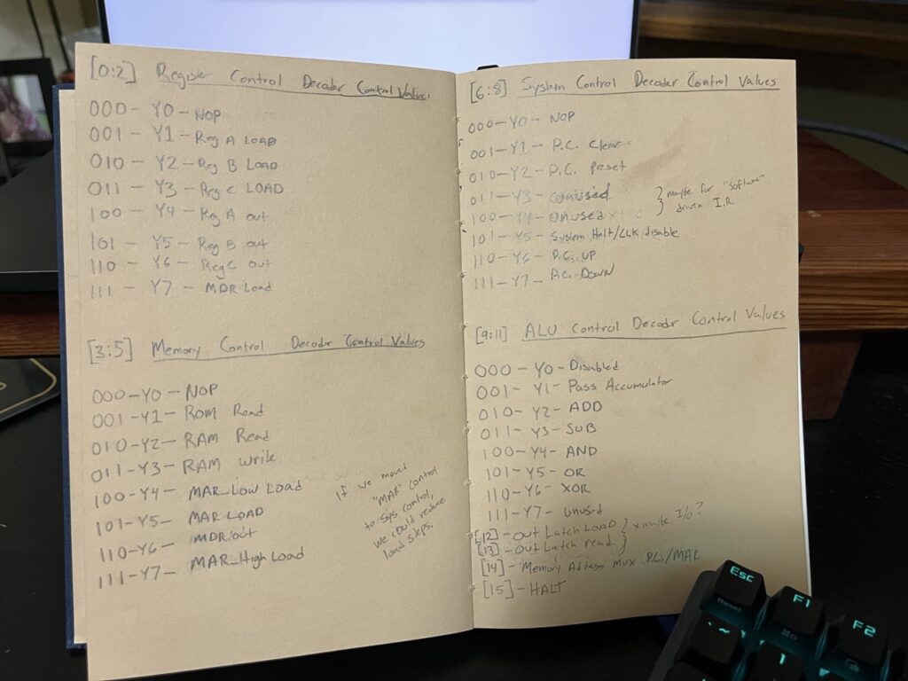
Control Word Architecture Implementation
16-Bit Control Word Structure
The control word architecture emerged from systematic analysis of functional requirements rather than arbitrary bit assignment:
[15] - System Halt
[14] - Memory Address MUX [1 = PC, 0 = MAR]
[13] - Output Latch Read Enable
[12] - Output Latch Load Enable
[11:9] - Decoder Bank 4: ALU Operations
[8:6] - Decoder Bank 3: Program Counter Control
[5:3] - Decoder Bank 2: Memory Operations
[2:0] - Decoder Bank 1: Register Operations
Decoder Bank Organization
Bank 1 [2:0] – Register Operations:
- 000: NOP
- 001: Register A Load
- 010: Register B Load
- 011: Register C Load
- 100: Register A Output Enable
- 101: Register B Output Enable
- 110: Register C Output Enable
- 111: MDR (Memory Data Register) Load
Bank 2 [5:3] – Memory Operations:
- 000: NOP
- 001: ROM Read Enable
- 010: RAM Read Enable
- 011: RAM Write Enable
- 100: MAR_LOW Load
- 101: MAR Full Load (16-bit)
- 110: MAR_HIGH Load
- 111: Reserved
Bank 3 [8:6] – Program Counter Control:
- 000: NOP
- 001: PC Clear
- 010: PC Preset
- 011: Unused
- 100: Unused
- 101: System Halt/Clock Stop
- 110: PC Increment
- 111: PC Decrement
Bank 4 [11:9] – ALU Operations:
- 000: ALU Disabled
- 001: Pass Accumulator
- 010: ADD Operation
- 011: SUB Operation
- 100: AND Operation
- 101: OR Operation
- 110: XOR Operation
- 111: Reserved
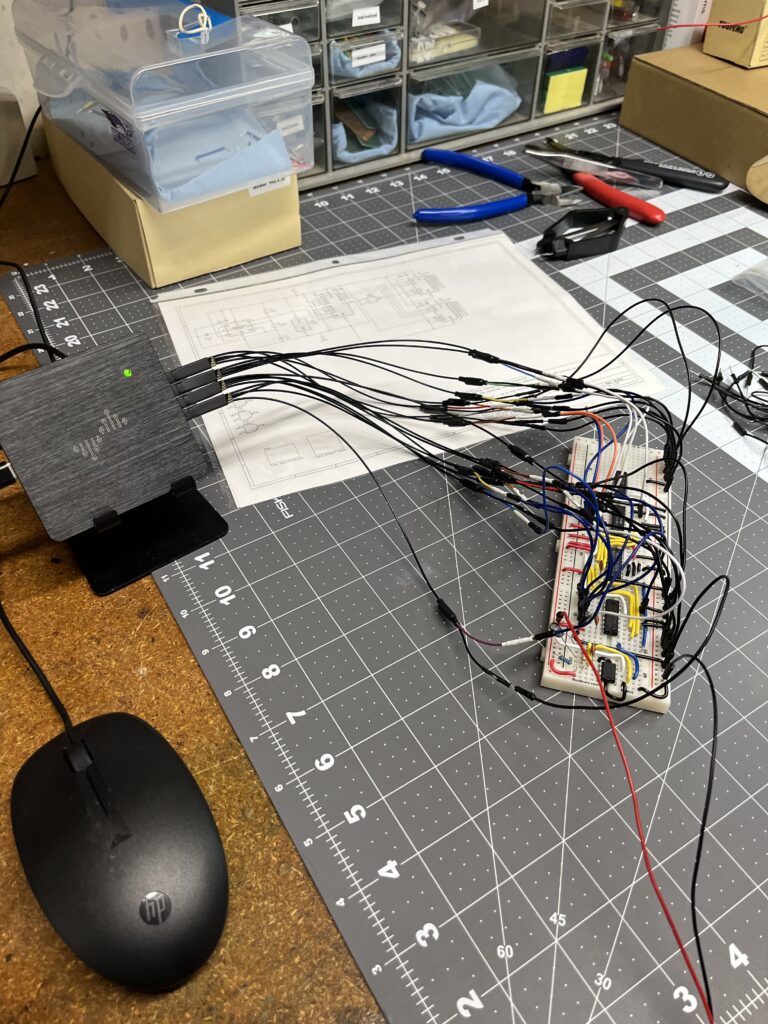
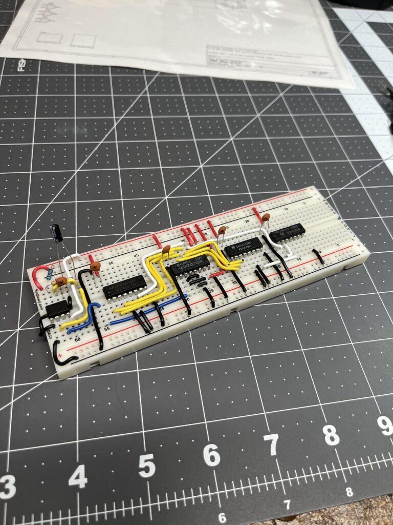
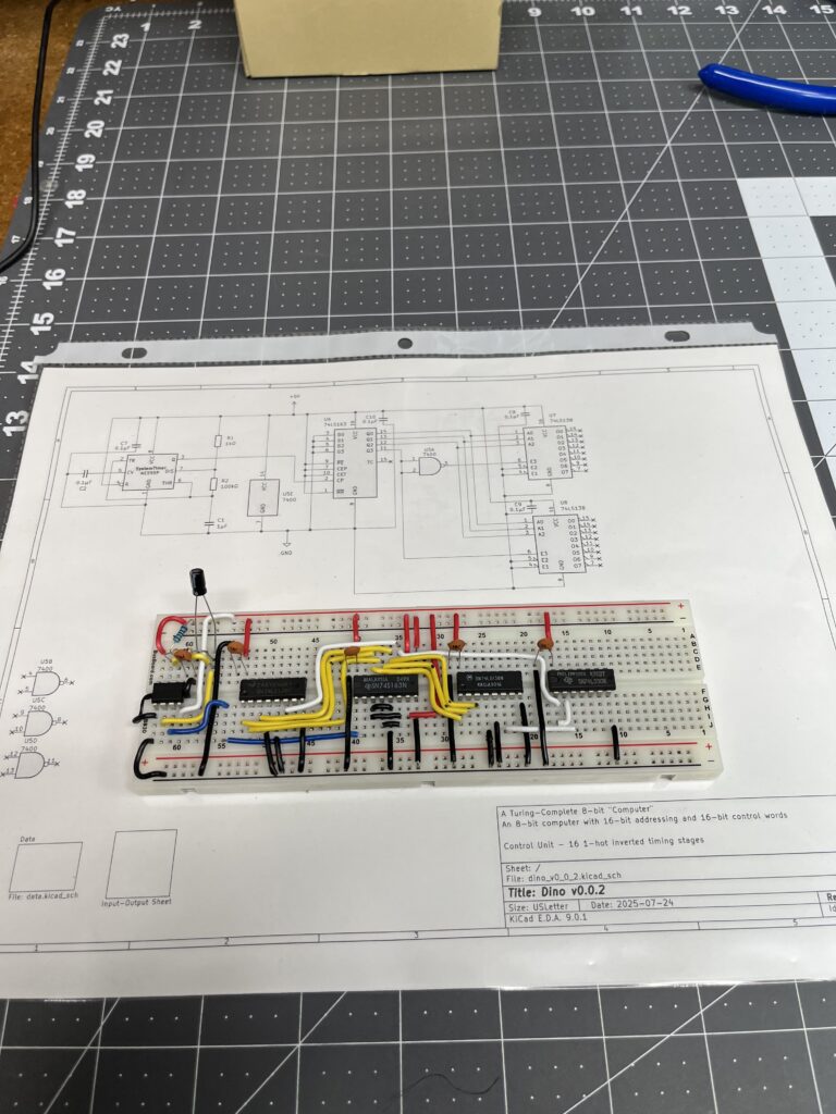
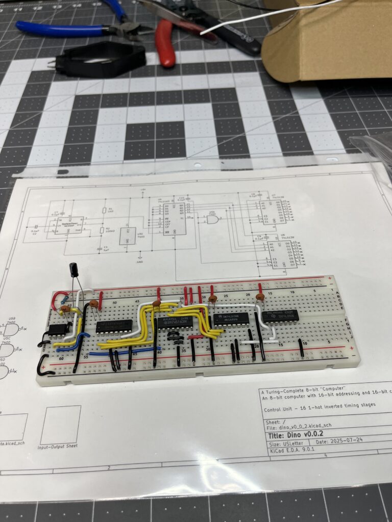
Ring Counter Architecture: 16-State Implementation
Design Requirements
Analysis of the instruction set revealed that 8-state operations (STA, STB) required a 16-state timing architecture. The design provides sufficient timing states for complex multi-word instructions while maintaining systematic timing coordination.
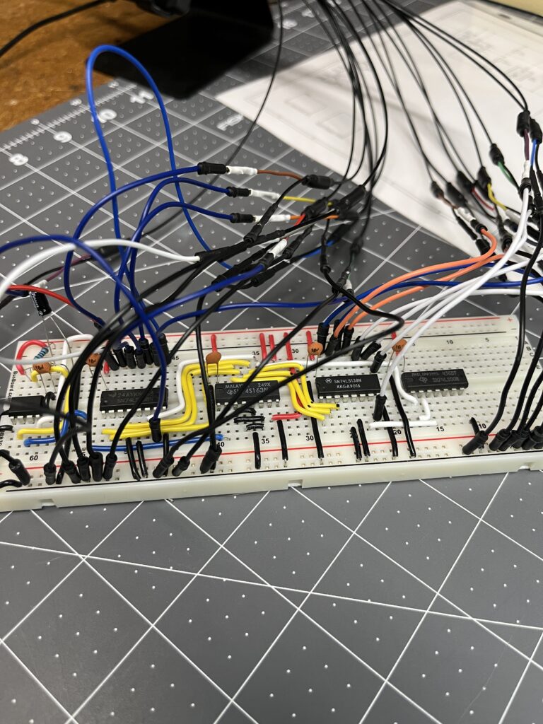
16-State Ring Counter Implementation
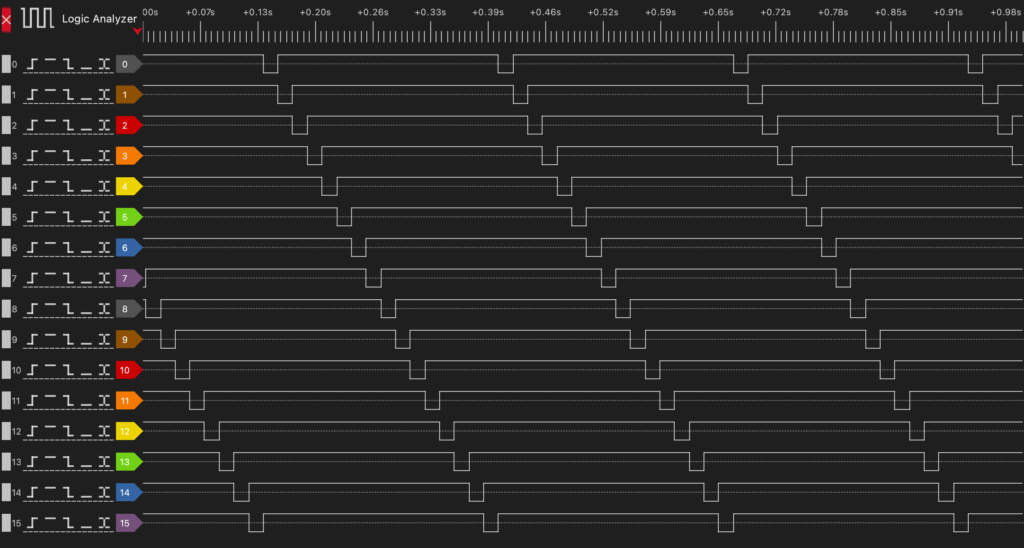
Architecture Complete: The 16-state ring counter has been successfully implemented and validated with logic analyzer verification.
Implementation Details:
- 74LS163 4-bit counter provides binary sequence 0000-1111
- 74LS138 Decoder #1: QD inverted via 74LS00 NAND gate (active-low enable)
- 74LS138 Decoder #2: QD connected directly (active-high enable)
- Natural reset: Counter automatically restarts at count=16 (0000 state)
Decoder Configuration:
- Decoder #1: Active during T0-T7 (QD=0, inverted to enable)
- Decoder #2: Active during T8-T15 (QD=1, directly enables)
- Complete T0-T15 timing sequence achieved
- Clean state transitions validated via logic analyzer
Instruction Set Implementation
Basic Load Instructions
LDAI (0x11) – Load Accumulator Immediate
T0: Universal - OpCode to MAR, MAR to IR
T1: Universal - Store PC in MAR
T2: Universal - Microcode branch point
T3: ROM Read, MUX=PC, MDR Load, PC Increment
T4: MDR to Register A
T5: NOP (instruction complete)
LDBI (0x12) – Load B Register Immediate
T0-T2: Universal fetch sequence
T3: ROM Read, MUX=PC, MDR Load, PC Increment
T4: MDR to Register B
T5: NOP (instruction complete)
Memory Store Instructions (8-State Operations)
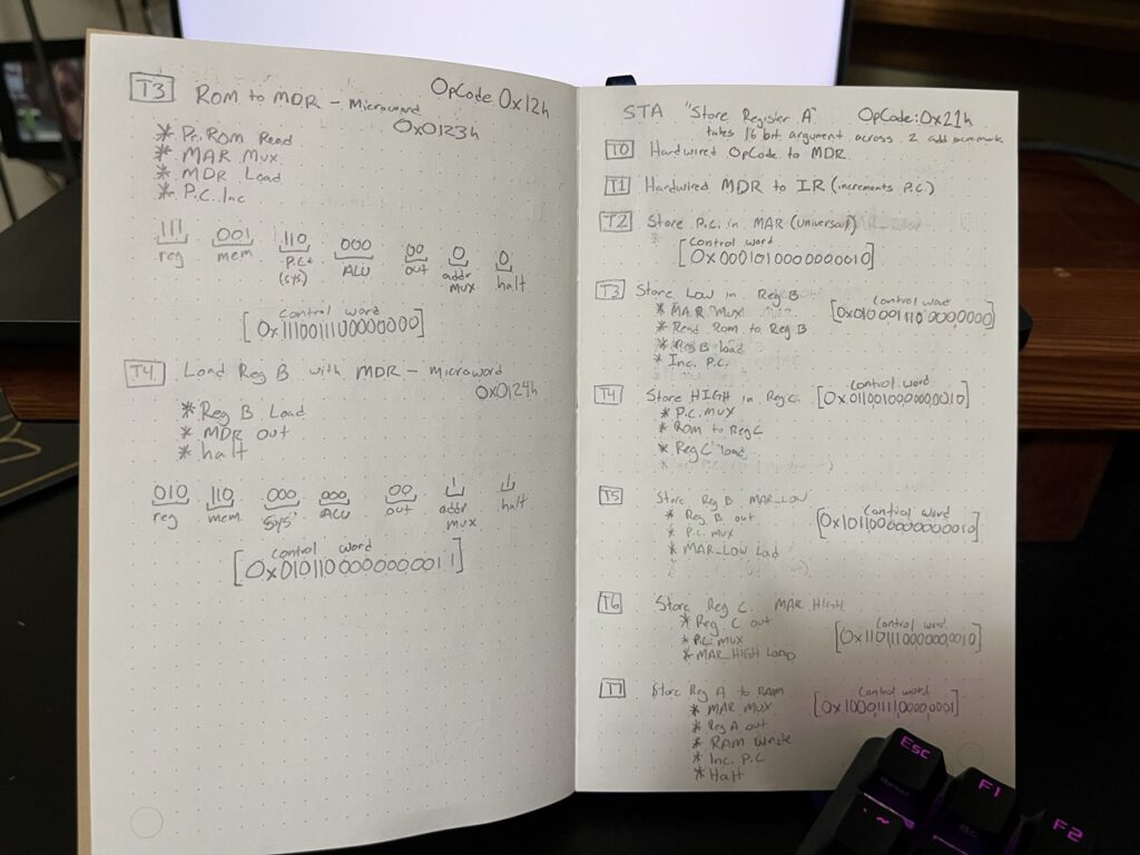
STA (0x21) – Store Accumulator to Address
T0-T2: Universal fetch sequence
T3: ROM Read, MUX=PC, Store address LOW byte to Register B, PC Increment
T4: ROM Read, MUX=PC, Store address HIGH byte to Register C, PC Increment
T5: Register B to MAR_LOW
T6: Register C to MAR_HIGH
T7: Register A to RAM via full MAR address
STB (0x22) – Store B Register to Address
T0-T2: Universal fetch sequence
T3: ROM Read, MUX=PC, Store address LOW byte to Register A, PC Increment
T4: ROM Read, MUX=PC, Store address HIGH byte to Register C, PC Increment
T5: Register A to MAR_LOW
T6: Register C to MAR_HIGH
T7: Register B to RAM via full MAR address
Test Program Development
Comprehensive Instruction Validation
LDAI 0x0D      ; Load immediate value 0x0D into Register A
LDBI 0x02      ; Load immediate value 0x02 into Register B
STA 0x0001     ; Store Register A contents to RAM address 0x0001
STB 0x0002     ; Store Register B contents to RAM address 0x0002
NOP            ; No operation (timing alignment)
LDA 0x0002     ; Load from RAM address 0x0002 into Register A
LDB 0x0001     ; Load from RAM address 0x0001 into Register B
ADD            ; Perform addition: A = A + B
MOVAC          ; Move result from Accumulator to Register C
OUT C          ; Output Register C contents to display
HLT            ; Halt system operation
Program Analysis
This test program validates:
- Immediate value loading to registers
- 16-bit address formation and memory storage
- Memory-to-register data retrieval
- Arithmetic operation execution
- Register-to-register data movement
- Output interface functionality
- System halt behavior
Engineering Insights and Optimization
Decoder Bank Strategy
The four-bank decoder organization emerged from systematic analysis rather than arbitrary grouping. Related control functions were grouped to minimize decoder complexity while maintaining functional separation.
Timing Domain Considerations
Operating at 60Hz provides generous timing margins for current implementation. Future optimization opportunities identified:
- Parallel control bit activation across multiple decoder banks
- Pipeline optimization for multi-cycle instructions
- Critical path analysis for maximum frequency operation
Memory Interface Architecture
The MDR (Memory Data Register) implementation proved essential for complex addressing modes. The MDR serves dual purposes:
- Temporary storage during 16-bit address assembly
- Data buffering for memory read/write operations
Architectural Validation
Control Word Matrix Verification
Each instruction’s control word sequence was systematically verified against datapath requirements:
- Register enable/disable coordination
- Memory read/write timing
- Bus arbitration conflict prevention
- ALU operation sequencing
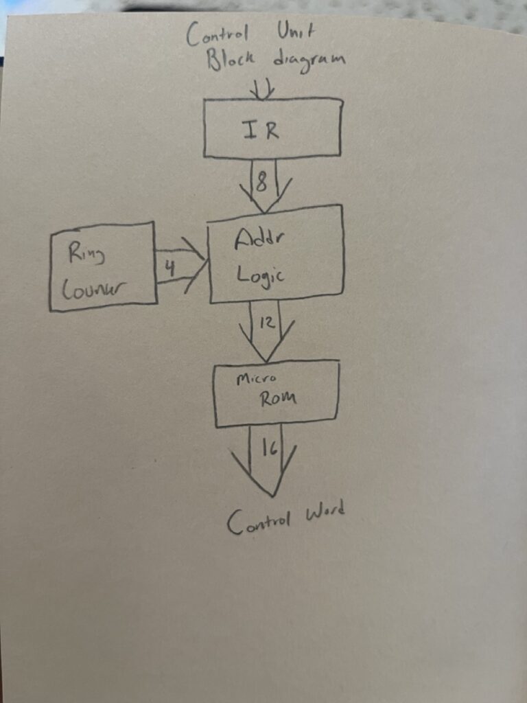
Universal Timing States
T0-T2 states implement universal fetch-decode operations:
- T0: OpCode fetch from ROM to Instruction Register
- T1: Program Counter storage for address reference
- T2: Microcode branch point for instruction-specific execution
This universal timing foundation enables systematic instruction expansion while maintaining consistent fetch behavior.
Project Status and Next Steps
Completed Implementation
- 16-bit control word architecture validated through systematic analysis
- Four-instruction basic set implemented with complete microcode timing
- 16-state ring counter constructed and logic analyzer validated
- Comprehensive test program developed for instruction sequence verification
- Decoder bank organization optimized for functional coordination
Next Development Phase
With the control word matrix architecture validated and the 16-state ring counter operational, the project advances to complete CPU integration:
- Control word ROM programming with the complete microcode matrix
- Instruction register integration with the validated timing states
- Full datapath construction connecting registers, ALU, and memory systems
- System-level testing with the comprehensive instruction set
Engineering Methodology
This phase demonstrated the value of systematic architecture study before implementation. The methodical approach of:
- Literature review of established computer architecture principles
- Systematic analysis of instruction set requirements
- Theoretical validation before hardware construction
- Comprehensive testing through representative programs
This methodology produced a robust control word architecture that can accommodate instruction set expansion while maintaining timing predictability and decoder organization.
The discrete logic computer has evolved from timing foundation to computational capability through systematic application of computer architecture principles to TTL implementation.